The servo must be simulated because it is complementary to the input circuitNo servo has worked fine for me so far,
Hi
i have got my pcb.
i checked as you mentioned in post 2296 - check with the ohmmeter whether the copper surrounding all component pads is connected to the mass on both sides;
hopefully i understand you clear - normally i have no problems with the via´s between upper and lower side of the pcb.
i use your diagram from post 1280 to recheck which components are connected to GND. every thing is fine.
whats next?
next i have to check all components- lets start with resistors. i have 1% 0,6W dale and MRS25 for my other amps i built. FW M2, AA14, FX8, FH9, ACA premium....etc.. the rest i have to check.
as i go and read all pages from #1267 i am sure the key is to be very accurate in the values of the resistors and every hfe at all transistors. this amp is
to decide to keep or not to keep this amp i plan to use just 30-40V rail. i guess my 500VA or double 300VA 24V or 30VAC should be enough.
kr
chris
Attachments
topic BJT:
for the OPS i plan to use my Toshiba 2SC5200 / 2SA1943 in To264 housing. the hfe i have got some pairs the are fit very exactly.
my other BJT transistors VAS are more problematic i guess. MJE15029G (about 390-430) and MJE15028G (100-150) are very bad for that...
for the IPS i have no problems - 5401/5501, or BC55x, ZTX851 /951
kr
chris
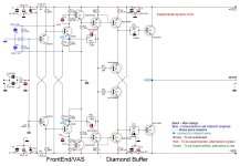
I am old school, I don't know what IPS/OPS stands for, however, I guess it is from the transistors you say. You better use a Peak DCM75 to match the transistors, even if the feedback puts everything in place. Surely the diamond buffer needs well-matched transistors because it is out of the feedback loop. T5 and T6 do not need to be cooled and can be even 2N5401/5551 if my memory doesn't fail.
I am old school, I don't know what IPS/OPS stands for, however, I guess it is from the transistors you say. You better use a Peak DCM75 to match the transistors, even if the feedback puts everything in place. Surely the diamond buffer needs well-matched transistors because it is out of the feedback loop. T5 and T6 do not need to be cooled and can be even 2N5401/5551 if my memory doesn't fail.
yes...
all my small transistors are match which warming lamp and DCA75 pro.
bigger transistors and Power MOSFET are match like Nelson Pass show us in his document.
i give them on a warmed heat sink (50°C) and test them with 5 different current values.
thank you
chris
Thank you for explaining.
I remember now I used all full plastic TO220 transistors for my application. However, I was forced to use an xVbe to prevent the thermal runaway since I configured the diamond buffer as a triplet. With the pure diamond buffer, no xVbe is needed, because the driver transistors sense the heat and prevent the runaway. So perhaps the full plastic TO220s are a good choice only for the CCSs, but not for the drivers.
I remember now I used all full plastic TO220 transistors for my application. However, I was forced to use an xVbe to prevent the thermal runaway since I configured the diamond buffer as a triplet. With the pure diamond buffer, no xVbe is needed, because the driver transistors sense the heat and prevent the runaway. So perhaps the full plastic TO220s are a good choice only for the CCSs, but not for the drivers.
Hi!
how important is the value of base stoppers R21,22=20 Ohm,
I forgot order them, may I use for example 10 Ohm or 100 Ohm?
I guess that voltage drop on them is marginal...
how important is the value of base stoppers R21,22=20 Ohm,
I forgot order them, may I use for example 10 Ohm or 100 Ohm?
I guess that voltage drop on them is marginal...
They set the bias of the driver stage and consequently the bias of the final pairs. You should not alter their value.
Hi,
I failed
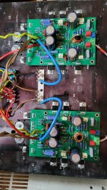
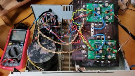
The amp burns positive rail fuses
Negative shows 100mA idle.
Please advice or drop the link for troubleshooting/startup procedure.
I used dead Denon pma920 enclosure and power supply
and a heatsink from french tank's radio (~3kg).
I failed
The amp burns positive rail fuses
Negative shows 100mA idle.
Please advice or drop the link for troubleshooting/startup procedure.
I used dead Denon pma920 enclosure and power supply
and a heatsink from french tank's radio (~3kg).
Attachments
Did you buy the MJE1503x on eBay? If so you got fakes for sure, they do not stand the nominal voltage of the amp.
The correct assembling sequence would be to populate only the VAS and check the voltage at the midpoint Q7/Q8 around 0V.
Then populate the two CCSs and verify more or less 137mA.
Then connect the drivers and the final pairs with their resistors.
All measurements must be done with a variac until you reach the nominal voltage.
The amp will be alive already at 4+4Vdc.
I wouldn't use any coil around Q1/2/3/4.
Thank you!
The parts are from tme so no fakes expected, however I didn't make good hfe matching.
The coil is grounded, do you think there is a risk of rf picking or other issue?
The parts are from tme so no fakes expected, however I didn't make good hfe matching.
The coil is grounded, do you think there is a risk of rf picking or other issue?
If the coil is grounded, it should be ok.
The MJE1503x are close to impossible to match, their NPN/PNP hFE is very different. However, your problem is elsewhere.
The PCB is very delicate, once a component is mounted, it is hard to desolder without damaging the PCB. Using a desoldering gun it is a lot easier, but still you have to pay attention. To experiment with this amp you should have some spare PCBs.
The schematic in my post #2107 shows the transistors I used.
Try to desolder one end of R21 and R22, and measure the voltage at the collectors of Q7/Q8, if it is close to 0V you are lucky and halfway to solving the issue. If the fuse still blows, you must exclude the CCS, the driver, and the final stages and retake the voltage Q7/Q8.
The goal of my suggestion is to be sure the VAS works properly. However, disconnecting R21 and R22 causes the final pair to saturate because they are driven by the CCSs, and both fuses will blow. To avoid this behavior you should disconnect R21 and R22 from the collectors of Q7 and Q8, then connect R21 and R22 free leads together. In this way, you turn on the drivers avoiding the final pair from saturating. If one or both fuses still blow, you must check the power stage first.
- Home
- Amplifiers
- Solid State
- Dartzeel amp schematic - build this?
