
I think that this will be better if you map the cut onto the PCB rather than the schematic.I don't see any reason why this will not work. Sections are complete splitted. Just values of resistors should be the same in both sections.
Attachments
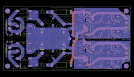
Yes schematic can be split, but you're wondering whether the PCB can be split, and PCB != Schematic. No one is saying thay schematic can't be split, rather that PCB cannot be split. Try to draw the line you need on the PCB and I believe you will find it difficult. I believe it's possible with 3 cuts and 2 jumpers (maybe 3?) (And sacrifice fuse) to get what you want.
Got to work at the correct level of abstraction.
green is cut, blue is jumper, red is where crc is now messed up.

Got to work at the correct level of abstraction.
green is cut, blue is jumper, red is where crc is now messed up.
Last edited:
You can see above, i made a cut and it works. Quite well 🙂 Only i would use dremmel this time instead of scalpel to cut it.
Did you find a simpler solution Brijac? Can you post a photo with a line where you found the cut?
Simpler is to make a custom pcb for your needs 🙂 Or make it on a peoto board.
You can clearly see the line where it needs to be cut. It doesn't need to be perfect. You get 5 pieces when you print out at jlcpcb. Discard the other half.
You can clearly see the line where it needs to be cut. It doesn't need to be perfect. You get 5 pieces when you print out at jlcpcb. Discard the other half.
clearly 🙄
I think what you're saying is that: when you get pcb's you get 5, so there is no need to turn the negative half into a positive half because there will be extra boards either way? if so I 100% agree
I think what you're saying is that: when you get pcb's you get 5, so there is no need to turn the negative half into a positive half because there will be extra boards either way? if so I 100% agree
Exactly 🙂 Also ldo's are not the same pinout. So it would be too much of a hassle. Much better solution is to make a custom board. I think i designed one for +V, but never peinted it, as this solution worked for me. I'll check and post if i find gerber.
Last edited:
Cannot edit previous post but I think this would get you two positives.
green is cut, blue is jumper, I am unsure of if this matters, but yellow is where r4 may need to be moved to.
A fun puzzle but I definitely agree with brijac that just using another pcb is best.

green is cut, blue is jumper, I am unsure of if this matters, but yellow is where r4 may need to be moved to.
A fun puzzle but I definitely agree with brijac that just using another pcb is best.
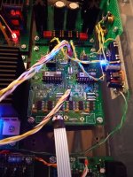
Here is the AD1862 finally in operation. The device is definitely in the range of PCM63.
At the start, it did not work immediately, because pin 8 on the I2S connector is not connected to GND, even if it is marked as a GND. Connected it from the bottom with pin 7 (also marked as a GND) and now everything is as it should be.
That I2S connector of mine is the same for all DACs (2-4-6-8 pins), so if pin 8 is not on GND, it won't work. Miro said he corrected everything, maybe we used an old gerber file? But all the same, it's nothing dangerous, it just won't work well, it screams.
So everyone who has a PCB for AD 1862, pay attention to that detail, so it's not a bad idea to check it while filling out the PCB.
Attachments
Hi,
looking forward to read your feeling after a longer breaking in as ast time I heard pcm63 it was not in a close layout with the ad1862 (which I like most)
Did you use the op1611 here as well ?
I think you will se the the little pcm54 is not ridiculous...
looking forward to read your feeling after a longer breaking in as ast time I heard pcm63 it was not in a close layout with the ad1862 (which I like most)
Did you use the op1611 here as well ?
I think you will se the the little pcm54 is not ridiculous...
I put the OPA1611 for a test, and then the heavier artillery will go. And I have to compare it to the PCM 63 because I'm interested in that too. The power supplies are always the same, the OPAs are the same, the capacitors on the DAC boards are the same, PCB designer is the same person, so it's a fair comparison. As the PCM 63 is now a rare beast, the AD1862 is probably the first choice.
It will not run at 384kHz sampling rate and was sourced from Rochester. 😳
The AD1865 and PCM1702 from China run the 384 like dragons. 🤣
The AD1865 and PCM1702 from China run the 384 like dragons. 🤣
@NIXIE62 I look forward to hearing your assessment/comparison. I am loving the PCM63/Sparkos. My 1862 has tubes, so not a good comparison of the ICs.
Quick question. I put in 1.2k IV resistors with the PCM63 and could use a little more gain. My pre has a buffer configured for no gain. Are there reasons for increasing the gain at the DAC vs the pre?
Quick question. I put in 1.2k IV resistors with the PCM63 and could use a little more gain. My pre has a buffer configured for no gain. Are there reasons for increasing the gain at the DAC vs the pre?
Since active classical I/V with OPA forms a virtual GND for the DAC chip, and it practically does not know what is happening behind it, feel free to increase that resistor. With 1k2 you have 1.7VRMS, with 1k5 you have 2.1VRMS with 2k you have 2.8VRMS. The calculation is simple, R (in kohm) x Iout (in mA) x 0.707=Vout (in V RMS). For PCM63 Iout is 2mA, for AD1862/1865 is 1mA, for PCM1702 is 1.2mA and for PCM56/PCM61/AD1856/AD1860 is 1mA.
Last edited:
Love to see flying metal!! 😉
Looking forward to seeing your completed MiroDac 6L6, enjoy!
Happy Holidays To All!!
Looking forward to seeing your completed MiroDac 6L6, enjoy!
Happy Holidays To All!!
- Home
- Source & Line
- Digital Line Level
- DAC AD1862: Almost THT, I2S input, NOS, R-2R