Rpi and Wiim are redundant, i.e. they do the the same ?
So I do not know w/o more information and picture of what you want to acheive it is not clear to me.
About the Rpi, this time : yes the generic i2s of the Rpi is flawed, so plug a reclocker with isolation in between, or if the streaming from it can be plugged on USB then uses JLSounds or Wave I/O USB to I2S - so via the USB streaming output of the Rpi or Wiim-
easiest for the Rpi is the FifoPi family from IanCanada. But you also can use the kali reclocker. With the Kali you will have pain to make clean 3 lines is2 grounded output because it has not ufl plugs the FifoPi has. Anyway Miro's board have I2S wires inputs vias too, it is just the ufl cables are better cause they are shielded and the ground follows the rigth paths for each line and it is plug & play (no soldering or shorts)
I do not understand how Wiim is outputing I2S, so I do not know, but there is no problem if it streams PCM through the USB or Toslink if the third party reclocker has either toslink and usb inputs.
Do not know if this is what you asked?
Last edited:

If I want to use separate PSU2 (modified to get 2x +-5V) only for Jlsound. Is it OK to have common ground for analog and digital part. Or cut pcb conductor to get totally separated psu?
two separate reg boards or the galvanic isolation will not work. The digital and analog must not be feeded by the same rectifying cap.
Best is to use a standalone traffo secondary for the digital side of the USB to I2S board.
Best is to use a standalone traffo secondary for the digital side of the USB to I2S board.
Will not be feeded by the same caps. Idea is to complete divide positive sides on PSU2. I've checked PCB so it is possible.
Then I will use 2 transformers. Nothing will be common between them except 220v input.
Then I will use 2 transformers. Nothing will be common between them except 220v input.
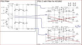
are the two outputs do not share the same pair of rectifying input caps on the PSU 2 board (see picture on the link below)? But perhaps I do not remember well, for me the two positive voltages at the output of the board share the big rectfying cap and snuber before but I could be wrong. Ignore my post if so.
https://www.diyaudio.com/community/attachments/20220526_181213-jpg.1058291/ : I putted a simple +5V (of a good quality, the white tiny board) for the digital side of the usb to i2s board (the red Wave I/O here in spite of the JLSounds but same phillosophy)
https://www.diyaudio.com/community/attachments/20220526_181213-jpg.1058291/ : I putted a simple +5V (of a good quality, the white tiny board) for the digital side of the usb to i2s board (the red Wave I/O here in spite of the JLSounds but same phillosophy)
Last edited:
There are 4 caps. 2 caps for 5v and 2 for 12v. If I cut connection between them I will get 2 grounds. One ground will be really ground for the first 5v and second will be positive +5v for second. Of course 12v part will be populated with the same resistor values as first +5v. I'm not sure if I was clear.
Two caps with resistor form a CRC filter for the negative rail (-12V, -5V) same for the positive rail (+12V, +5V).
If you want separate power supplies, with independent transformer secondaries, this board will not work for you no matter what you propose to cut.
If you want separate power supplies, with independent transformer secondaries, this board will not work for you no matter what you propose to cut.
As far as I remember, when you cut the PSU2 in half, you can make one + regulator and one - regulator on those cut PCBs.
Yep. I use it like that. Separate secondary is of course needed.As far as I remember, when you cut the PSU2 in half, you can make one + regulator and one - regulator on those cut PCBs.
One note, i would use dremel and cut it. I tried scoring with scalpel and it was a painfully long process.
There is a link in the first page on the Miro mini site.Subscribed. But why not a nice tube output stage for this DAC instead of opamps?
Yes exactly. I need 2 positive 5v for Jlsound. One for digital and second for analog section. As I have spare psu2 pcb's idea is to use them.
As far as I remember, when you cut the PSU2 in half, you can make one + regulator and one - regulator on those cut PCBs.
I do not think so as at the end you have two +-0- , one on each half side, you can not divide it by half to make two polarities, and whatever you do on the same polarity, it is shared from the beginning so it is not working when you need galvanic isolation.
So the answer is NO, you can not use a same PSU2 board to feed the digital and the analog side of the JLSounds if you want to do it to profit of the galvanic isolation. Vunce explained why.
Last edited:
Hi guys. Can I ask for some help please?
So today after a long time of no Miro DAC in my system I put it back in. It's a Ian Canada /RPI front end. The dac that was there was one of Richard's excellent little dacs.
So all I did was swap the dac and PSU dac out, now in there is my long term tested PSU1 and Miro 1862. Obviously had to switch the i2s and outputs.
All I can get out is LOUD highly distorted music. Even with the digital volume down and the preamp knob on 1 click, I get pretty loud distorted music.
The Miro 1862 has the same PSU, transformer as in the other chassis. It is just getting a different i2s source. (from Ian's fifo.) I've double checked the i2s as I'm aware the labelling is slightly different between the dac and the fifo but think I'm all good there.
Have turned off any oversampling in the Rpi so I'd getting the native sample rate. Clock lock lights illuminated so that's working. Checked opamp orientation.(1611)
Anyone had anything similar or what to check please?!
Last edited:
You can certainly cut the PSU2 board in half and make one positive (+5V) and one negative regulator (-4V). With the negative supply -4V, you just ground the minus output to the chassis via 100nF and use it for the JLS XMOS part. It is only important to have a separate secondary on the transformer for the XMOS part, galvanically separated from everything else, and to cut the GND jumper on the underside of the JLS board. And also two PSU2 boards can be cut and only two positive parts can be used. One +5V 100mA and one +4V 400mA. XMOS regulator must have large heatsink.I do not think so as at the end you have two +-0- , one on each half side, you can not divide it by half to make two polarities, and whatever you do on the same polarity, it is shared from the beginning so it is not working when you need galvanic isolation.
So the answer is NO, you can not use a same PSU2 board to feed the digital and the analog side of the JLSounds if you want to do it to profit of the galvanic isolation. Vunce explained why.
Feedback
When you cut the PSU2 in two halves, you only have the option for what I said, one positive and one negative regulator. Besides, you need room on PCBs for bigger coolers, especially for the XMOS part.
The negative regulator can also be used, (LT3015) just ground minus output to chassis with 100nF and provide a separate secondary. Use that for XMOS. 4V DC is enough, to reduce the heating of BD139 on the JLS card. Adjust the resistor values of LT3015 for 4V output. It's all tried and it works.
The negative regulator can also be used, (LT3015) just ground minus output to chassis with 100nF and provide a separate secondary. Use that for XMOS. 4V DC is enough, to reduce the heating of BD139 on the JLS card. Adjust the resistor values of LT3015 for 4V output. It's all tried and it works.
Last edited:
- Home
- Source & Line
- Digital Line Level
- DAC AD1862: Almost THT, I2S input, NOS, R-2R