Here are the LRCK and CLK at 384K directly on AD1862 pins, no input from computer but USB connected. The data line pin is null as should be. You can confirm the frequency


So, I think the wave is not overshooted. My scope is only 60Mhz so, take it also into account. Do you think still better to add small series resistance to lines to AD1862. On PCB we have place to install smd resistors.
I was thinking on increasing capacitance on NR1 and NR2. Currently, I have 47uF and 4.7uF.
I have 3 parallel AD1862 (Iout in parallel). Each floor has its own capacitors above. Only share same voltages, but each have it's own 0.1uF decoupling near pins for digital and analog voltages.With one floor the situation is the same (LRCK residuals with no input).
I have 3 parallel AD1862 (Iout in parallel). Each floor has its own capacitors above. Only share same voltages, but each have it's own 0.1uF decoupling near pins for digital and analog voltages.With one floor the situation is the same (LRCK residuals with no input).
Exactly what I just thinking. There is a leakage into I/V which is filter-less! It amplifies the tiny current. I will check with scope the Iout directly on DAC pin. If the scope can't detect anything it means the I/V amplifies this little induced current the scope can't show.
I tested the AD1862 Iout line with scope. I don't see LRCK hints. I tried to amplify the line before the scope (60db LNA and put the LRCK on 44.1K, amplifier bandwidth wide enough), but mainly see noise, can't say it is 44.1k... Anyway, I am sure it is a leakage to I/V anyway and as you said (Bohrok) no LP so I can see it even with scope.
It might be interesting to someone, the device shows the sampling frequency of the audio signal. In order for it to work, it needs to be connected to LRCK, +5V and GND.
https://vi.aliexpress.com/item/1005002981762996.html?gatewayAdapt=glo2vnm
https://vi.aliexpress.com/item/1005002981762996.html?gatewayAdapt=glo2vnm
Most of the XMOS-based devices does not stop WCLK and BCLK at "stop", just keep SData at 0 (or 0x9696 for DSD) and provides additional "mute" signal.It seems the I2SOVERUSB does not stop when no music is played.
Yes, also, in modern DAC you can't measure noisefloor directly as it has internal mute, on chip or by relay or both. One can estimate the noisefloor by THD+N at low levels (like -60dbfs). I mean that I arrive this problem (of seeing LRCK residuals) mainly as I am using AD1862 plainly without LP.
@gaycoh I measured this LRCK residuals also on the PCM1704 (without filter) with galvanically isolated digital inputs. It is few years old measurement, just found it in my PC 😆 From the PCM1704 it is much worse than from the AD1862. It can be filtered with the LP filter, or let it be if it is not audible 🙂
5mV digital noise from 1.2mA current (1k5 I\V resistor) = it is 3.3uA "glitch".
5mV digital noise from 1.2mA current (1k5 I\V resistor) = it is 3.3uA "glitch".
Attachments
Thanks Miro,
I am using I2SOVERUSB in fully isolated mode (clean and dirty).
I took my other Agilent scope to capture (it has this MegaZoom so can dig better). The problem, is a

 CRT so hard to catch by a digital camera (scanning issues).
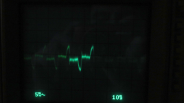
Anyway, I have 3 parallel floors of AD1862 with 1kohm conversion resistor. I could remove two floors and see if the glitch is reduced by a factor of 3. More or less this is the situation. In the following pictures you can see two shots (44.1k Fs). One with 3 floors (of AD1862) and one with 1 floor. Resistor is of course fixed 1kohm. I put the cursors and you can look at the delta Y (delta for offset nulling). With 1 floor it is 1mV, so basically 1uV at Iout which is 60db less from its full scale. More or less the proportion is preserved with 3 floors.
I am using I2SOVERUSB in fully isolated mode (clean and dirty).
I took my other Agilent scope to capture (it has this MegaZoom so can dig better). The problem, is a
Anyway, I have 3 parallel floors of AD1862 with 1kohm conversion resistor. I could remove two floors and see if the glitch is reduced by a factor of 3. More or less this is the situation. In the following pictures you can see two shots (44.1k Fs). One with 3 floors (of AD1862) and one with 1 floor. Resistor is of course fixed 1kohm. I put the cursors and you can look at the delta Y (delta for offset nulling). With 1 floor it is 1mV, so basically 1uV at Iout which is 60db less from its full scale. More or less the proportion is preserved with 3 floors.
In terms of bits, 1uA (before I wrote by mistake 1uV) is 10 bits. Is it really what is called glitch ? Major carry transition or we (me and you) just called it like that? I think it is a kind of problem coming from the AD1862 architecture of switching. The data is null in all my measurements (checked) so theoretically the internal DAC buffer should transfer 0 at LRCKs.
However, it doesn't. Maybe it is related to how the AD1862 is making it's switching where there is some energy in its capacitors. Maybe it is also related to the fact that the I/V doesn't really present 0 potential (virtual ground) to Iout.
Hence there is some bouncing between I/V input to DAC output internal network
From Wikipedia:
The I²S protocol outlines one specific type of PCM digital audio communication with defined parameters outlined in the Philips specification.
The bus consists of at least three lines:
In this case it should be like this:
SCK=BCK
LR/DO = LRCK
SD/01= DATA
GND=GND
MCLK is not used
The I²S protocol outlines one specific type of PCM digital audio communication with defined parameters outlined in the Philips specification.
The bus consists of at least three lines:
- Bit clock line
- Word clock line
- At least one multiplexed data line
- Master clock (typically 256 x LRCLK)
- A multiplexed data line for upload
In this case it should be like this:
SCK=BCK
LR/DO = LRCK
SD/01= DATA
GND=GND
MCLK is not used

- Home
- Source & Line
- Digital Line Level
- DAC AD1862: Almost THT, I2S input, NOS, R-2R