It is not like that simplified... First determine what is the ballanced line input sort off: transformer, OPamp other.
Then You can think of way to connect it with source?
Then You can think of way to connect it with source?
Here is the link. There are no transformers at the inputs.
Fully balanced class A design built by discrete analog stages without any OPA or coupling caps in the signal channels.
http://www.audio-gd.com/Pro/Headphoneamp/NFB1AMP/NFB1AMPEN.htm
Fully balanced class A design built by discrete analog stages without any OPA or coupling caps in the signal channels.
http://www.audio-gd.com/Pro/Headphoneamp/NFB1AMP/NFB1AMPEN.htm
@EUVL posted a layout for a small footprint AD797 passive IV converter in post 6316
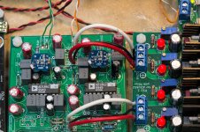
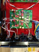
Today I got to make up a set for my test DAC build. There are very few parts, and once you are comfortable with SMD soldering the build is easy. It is a direct drop in to the DAC, but you must remove Riv and Civ from the board if you have them fitted. Very neat, low cost, runs from the supplies on the @miro1360 board, or you can supply a separate 12V by using the jumpers on the DAC board.
Very useful, excellent for anyone wanting a small footprint but also wanting to try passive IV. Listening impressions to come later.
Fran
Attachments

Here the Gerber files and the BoM :
1x IC1 AD797 SOIC8
facing downwards
1x Riv Susumu 0805 27R 0.5%
1x Rs Susumu 0805 27R 0.5%
1x Rf Susumu 0805 2.7k 0.5%
2x Cs Murata C0G 0805 10nF 25V
1x Civ Murata C0G 0603 2.2nF 50V (solder between Pins 2 & 3)
1x C8 Murata C0G 0603 51p 50V (for AD797 only)
Many thanks to Fran for verifying PCB.
Enjoy,
Patrick
Attachments
Thanks Fellas!
Of all the opamps I rolled in MiroDac, the AD797 has eluded me. I’ll give this a go.

Of all the opamps I rolled in MiroDac, the AD797 has eluded me. I’ll give this a go.
@NIXIE62 Today I almost finish with connection to XLR. I use the new pairs of wires for L and R channels and resistors. Red - signal wire and white - GRN. Red to the 2 pin and wht - 1 pin on XLR. Left resistor to the 3 pin and then to the GRN of left RCA. And what about right? Combine both resistors and connect to one GRN or I should choose different GRN for 3 pins?
Attachments
Try the ADA4625-1, but just as an I/V, not as a passive. The sound is similar to the AD797😉Thanks Fellas!
Of all the opamps I rolled in MiroDac, the AD797 has eluded me. I’ll give this a go.
I don't consider DDDAC to be a superior dac, mainly because of the poor power supply - regulators and the absence of a real I/V stage.So it's similar to PCM63. I haven't tried it (passive I/V), maybe I will try it, maybe I won't, it depends on the hearing tests we will do with two or three variants of I/V. Currently in DDDAC I have a passive I/V and then a line transformer. I am very satisfied with the sound. Because of the high output current, nothing else is needed, no active stage. For something else to come along and replace the DDDAC, it has to sound better.
You can get a lot more out of only two PCM1794, you just need to read the TI application manuals.
Is it a theoretical consideration, or have you had the opportunity to hear a well-made DDDAC with 4 boards and Sowter output transformers, and compared it with a PCM1794 DAC made according to the datasheet? What does real I/V stage mean? DDDAC has a passive I/V (I/U) stage, considered by many to be superior to any active I/V (I/U).
Connect the right one the same as the left one, with separate resistor on Pin3 to the other output. It's all the same GND on the PCB.And what about right?
PS
By the way, I'm not sure what those resistors between Pin3 and GND are for. I would leave them out. When I made the XLR/RCA adapters, I connected PIN3 directly to GND. In this case it was a connection from an unbalanced preamplifier (RCA) to a balanced amplifier (XLR). I also bought two off-the-shelf connectors, and they were done the same way.
Last edited:
I use only 1-2 pins without 3. All output is working but need to listen carefully.Connect the right one the same as the left one, with separate resistor on Pin3 to the other output. It's all the same GND on the PCB.
PS
I'm a little confused, Pin 3 of each channel should be connected to GND in the DAC or in the cable (or in the adapter) XLR/RCA. The negative input of the preamp (pin3) should have a GND reference when the balanced input works as an SE? Probably there is a resistor in the preamplifier from each input to GND, so that's why it works, who knows?
I've consulted with several people and it should be connecting of the 3 pin (cold) with analog ground Dac. For 1862 it will be 12 leg (AGND) or I/V opamps leg ( Gnd - 3). It would be a differential signal for XLR. But I can't to solder (very uncomfortable). I don't want to disassemble everything including wires inside.
I think I will going the same thing with my 1865 but with 3 pin of XLR. I need to check the schematic but opapms leg is same - 3, only Dac legs are different. I recently ordered the second transformer and I don't have the XLR connectors for experiment.
Yesterday I carefully listened my upgrade through headphones and fully satisfied with the result!
@NIXIE62 Thanks for the answers!
You can connect PIN3 in the cable itself. That's what I did and it works. And so it is in the factory XLR/RCA adapter.
I know too. I was built a similar cable - rca to xlr. But there is a risk for some devices. I had heard the opinions that it is wrong. Anyway AD1862 is rare chips and you have to be careful with them.You can connect PIN3 in the cable itself. That's what I did and it works. And so it is in the factory XLR/RCA adapter
It would be interesting to compare differential signal and non from one device. At least - it should be louder.
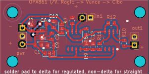
I've been wanting to try an OPA861 I/V but some of the parts Vunce used in #1417 have long lead times. I'm trying my hand at making my own pcb's and think these are ready to print, but I'd appreciate any feedback.
As for changes I replaced the TPS7A39 with an LT3032 and 6 pin 861's with 8 pin 861's because of availability. I also removed Vunce's C4 and C10 as per #2133. I decided to use the fixed 5v LT3032 as it seemed easier. I added some pads to see If I can hear the difference without on-board regulation as well.
Feedback is super appreciated!
I'll post other files if people want them, and am planning to post gerbers after I've tested the boards.
Attachments
- Home
- Source & Line
- Digital Line Level
- DAC AD1862: Almost THT, I2S input, NOS, R-2R