I have found the copy of the gerber files for Miro1862 DAC in earlier post and my question is: Can I use these files to have boards made? I am going by the fact that they are posted they are OK but I want to make sure. If so has anyone used them before successfully at any of the PCB build co. out there? Thanks for any feed back.
best regards,
Steve
best regards,
Steve
@hartbigsky Use gerber files from the first post, it is the best 🙂 There are another versions, mostly worked fine.
So it's similar to PCM63. I haven't tried it (passive I/V), maybe I will try it, maybe I won't, it depends on the hearing tests we will do with two or three variants of I/V. Currently in DDDAC I have a passive I/V and then a line transformer. I am very satisfied with the sound. Because of the high output current, nothing else is needed, no active stage. For something else to come along and replace the DDDAC, it has to sound better.100ohm is too much for PCM1702🙄
50 and below will be fine, 100 gives a soft sound, without kick and details in the middle, regardless of which tube is used
It's a pity to use PCM1702 like that and without a real I/V stage
Hi,
It's Lyuben from JLsounds.
Best,
Lyuben
It's Lyuben from JLsounds.
After reading AD1862 DAC datasheet more carefully - CLK is max(min17MHz), which means that it's possible to have some DACs on which maximum CLK frequency to drop to 17MHz, but it's not specified maximum CLK frequency, i.e. it may go to 30MHz, this means that some DACs may work on higher frequencies, some doesn't, i.e. it's guaranteed that all AD1862 will work up to 17MHz.I will check, you are right I should check it before. Just was taking the AD1862 datasheet as truth, see it is written support X16.
I actually don't know how the I2SOVERUSB work.
Is it 768k*20*2 or 768*32*32, in both cases it is higher than 17Mhz 🙂 so, in any case how they can write support X16 when the limit is 17Mhz?
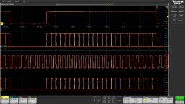
Your and other guys math is absolutely correct - 768k * 20 < 17MHz, but this means that the frame word must be 20 bits, in order all AD1862 to work on 768kHz, not 32 bits like JLsounds board outputs (768k * 32 > 17MHz). Here is oscillogram of bit depth for PCM1704, oscillogram for AD1862 is the same, but 20 bits 🙂AD1862 supports 16x but word length should be 20 (48*16*20 = 15.36MHz). Some digital filters can output 20bit word length.
Best,
Lyuben
Attachments

What is the difference between AD1860N-T and AD1860N-K. Which one is better? There are a lot of them on ebay for small money, I have a PCB for PCM56/AD1860, I can try that too.
https://www.ebay.com/itm/165480106432?hash=item26876209c0:g:ypQAAOSwhI9eqT-n
https://www.ebay.com/itm/165480106337?hash=item2687620961:g:ZoQAAOSwhjNeqT8g
N-T seems more original to me than N-K (at least on the picture). You know what they say for DAC chips, the older the better. 🤣
For whom interrested Pedja Rogic, is making an interest poll for the mk 3 version of his usb to i2s simultaneous mode card for the TDA1541A : 384 K hz feasible with two channels possible or 4 channels up to 192 k hz.
It was from a discussion by pm between me and him as I wanted 3 years ago a sota front end but with the vias arrengement to plug ANdrea Mori SC Cut adaptors. He didn't realised it in the AYA5 wanting to stay straithforward while was ok for a discrete outputstage I asked some profit now, but said he will see what is possible with a standalone front end. I pushed from the AYA 2014 edition to have uf-l plugs to have back then some freedom to plug the I2S PCM card from Iancanada and since the Aya is continuing with a good sucess for exigent diyers thanks to Shane Ceglar and CFT (Cheung) members that asked to Audial to re launch the Aya from an idea I had to ask a manufacterer due to some not succeding to work cleverly together here.
Up to you to make the story continuing, with the poll you can type a message with ideas, Rogic is an open guy. It is the oppurtinity to make a multichannel dac with tda1541A in sim mode with a sota layout from a guy that has 30 years of experience around that chip. https://www.audialonline.com/blog/usb-interface-board-mark-3/
Last edited:
Lyuben explained everything nicely. Some chips will work some won't at those high frequencies. It's just that I still don't understand what is achieved with 768kHz sampling rate, in terms of sound quality?
Guys, I want to use XLR output parallel to the unbalance (RCA). I don't need a true balance. So I know the next method:
- 1pin ground
- 2pin signal (L and R)
- 3pin ground with resistor that corresponds to the output on Dac board (100ohm)
Attachments
There is a known Pin1 issue. As a rule, pin1 for XLR connectors is connected to the chassis, and somewhere it is connected to the signal GND. How is your DAC GND connected to the chassis? Directly, indirectly via a NTC resistor or some other way?
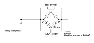
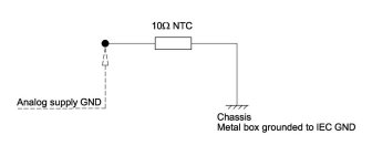
In your case I would try to connect Pin1 to the signal GND on the DAC board between the L&R outputs. And since you have a metal box, it must be connected to the IEC connector GND, and then the signal GND from the analog power supply is grounded to the chassis via gretz 10A+100nF+100ohm resistor or just with 10ohm NTC resistor.
In your case I would try to connect Pin1 to the signal GND on the DAC board between the L&R outputs. And since you have a metal box, it must be connected to the IEC connector GND, and then the signal GND from the analog power supply is grounded to the chassis via gretz 10A+100nF+100ohm resistor or just with 10ohm NTC resistor.
Attachments
Last edited:
If it's a plastic chassis, then what I wrote doesn't apply.
NTC 10ohm is usually placed from the signal GND to the grounded metal chassis. It is a GND Loop breaker, protection against too high touch voltage and removes electrostatic charge. Graetz rectifier 10A +100ohm+100nF has the same function (100nF is AC GND for high frequencies).
22ohm are the output resistors on L&R line outputs, they have nothing to do with grounding.
Last edited:
If your next device is balanced, then you have to connect pin 3 (-input, cold) to GND either in the DAC or in that device (preamp I guess). Obviously this should be done in DAC. When you connect it like that, the balanced device will have half the voltage gain (-6dB).
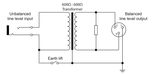
Another way is to use a line transformer to convert unbalanced to balanced. But it's not cheap.
Another way is to use a line transformer to convert unbalanced to balanced. But it's not cheap.
Last edited:
I have AudioGD NFB-1 amp. He is fully balanced. audio-gd Stellar product
What kind transfomer you mean?
What kind transfomer you mean?
Why don't you use RCA inputs?I have AudioGD NFB-1 amp.
Attachments
- Home
- Source & Line
- Digital Line Level
- DAC AD1862: Almost THT, I2S input, NOS, R-2R