@Markw4
4-layer or even 6-layer because of many different voltages 🙂 It's not a problem to create one.
Your suggestion to avoid ferrite beads is correct.
4-layer or even 6-layer because of many different voltages 🙂 It's not a problem to create one.
Your suggestion to avoid ferrite beads is correct.
@Hidy Thank you for all your hints 🙂
The stop-clock PCB contains gaps in the GND plane, between digital and analog, and GNDs are connected under DAC chips ... it can improve something, or maybe not, hard to say without testing 🙂
I still think these LDO regulators have big problem with capacitors. Can you test the 78/79xx regulators how they perform in comparison with the LDOs? 😀
Split ground planes are nice🙂
I don't have 78/79 regulators. I will order some to test sometime in future.
Hidy
@miro,
I ran pink noises for a whole night and I measured again. This time the left and right channels performed identical. It turns out that there is nothing wrong with the PCB layout for either channel. I confirmed the measurement results with both AD797 and Sparkolab SS3601. I have also found that SS3601 performs even better in the test, with THD down to 0.002780%.
View attachment RightMark Audio Analyzer test _ [DirectSound] miro ad1862 SS3601.pdf
Then I tested with Holo Titanis in the usb link. And I was surprised to find that the Titanis actually cleaned up a lot of my computer noises that got into the dac despite that I was using an isolated XMOS board.
Here is a graph to show how clean this dac can be once the usb noises are removed. The left two graphs are without Titanis. The right two, with Titanis.
 vs With Titanis (right).png")
Here is a complete report with Holo Titanis in the usb link.
View attachment RightMark Audio Analyzer test _ miro ad1862 ss3601 holo titanis.pdf
Cheers!
I ran pink noises for a whole night and I measured again. This time the left and right channels performed identical. It turns out that there is nothing wrong with the PCB layout for either channel. I confirmed the measurement results with both AD797 and Sparkolab SS3601. I have also found that SS3601 performs even better in the test, with THD down to 0.002780%.
View attachment RightMark Audio Analyzer test _ [DirectSound] miro ad1862 SS3601.pdf
Then I tested with Holo Titanis in the usb link. And I was surprised to find that the Titanis actually cleaned up a lot of my computer noises that got into the dac despite that I was using an isolated XMOS board.
Here is a graph to show how clean this dac can be once the usb noises are removed. The left two graphs are without Titanis. The right two, with Titanis.
Here is a complete report with Holo Titanis in the usb link.
View attachment RightMark Audio Analyzer test _ miro ad1862 ss3601 holo titanis.pdf
Cheers!
New findings.
This ad1862 DAC performs best with 44khz sampling rate. I tested 16 bit 44khz and got a THD of 0.00278%. Then I tested 24 bit 44khz and got a THD of 0.00271%.
16bit 44khz
View attachment RightMark Audio Analyzer test _ [DirectSound] ss3601 44.1.pdf
24bit 44khz
View attachment RightMark Audio Analyzer test _ [DirectSound] ss3601 24 44.1.pdf
I am happy about this since most of my music is in 16bit 44khz format.
Cheers🙂
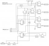
@jpk73 See the main board diagram on the first page (CDS3main_R4.pdf)
There is only one CLK common for both DACs, therefore it cannot be stopped.
PMD200 outputs dataL/R simultaniously to the DAC chips, and they share one clock. This clock comes from the stopped clock circuit. Simulation of the circuit showed that actually it does stop the clock. You don't need 2 clocks for stopped clock operation! PMD100 and other chips also output one stopped clock for both channels.
In the AN207 note stopped clock was designed to make R and L appear in sync. But later it was found that stopped clock improves noise as shown in diyinhks scope shots...
Last edited:
I still think these LDO regulators have big problem with capacitors.
Two things about LDO's: (1) they can sometimes be used with SMD film output caps instead of X7R, but its something that might require some measuring and tweaking with a scope to check for stability; and (2) LDOs sometimes sound better if the output is loaded with a resistor to ground. Since I typically run in 3.3v LDOs from a 5v input rail (maybe the 5v rail is pre-regulated with LM317), LDO power dissipation is usually low in that case. That means I can get away with dumping a fair amount of LDO output current into a load resistor to ground. For a 3.3v rail, sometimes I get good results with 47-ohm, 1/2-watt, metal film to ground.
Between use of film caps and loading resistors, LDOs can often be made to sound better. That's not to say they will ever sound as good as a purpose-built discrete regulator, but for clocks, DSP, ASRC, etc., they can work quite well. For analog audio circuitry power rails I would probably not use a super high performance LDOs. Don't prefer the sound of them myself for that purpose.
Last edited:
@Hidy Thanks for your findings and how deep are you going with testing 🙂 Seems like my DAC performs very good 😀
@jpk73
It means, DL and DR are aligned internally in the PMD200 chip for one clock.
@miro1360: that's what most DF chips do. So it seems stopped clock logic is not needed for aligning channels if used after a DF, but for reducing noise it's still very interesting. Also it could be worth to reclock LE before the DAC chips. But maybe that's a different application than what you had in mind...?
Last edited:
@jpk73 Aligning I2S DATA with stopped clock logic that way needs a lot of glue logic (or CPLD, which only a few can program at home 😀). If I come up with something simple, I'll make a diagram 🙂
@jpk73 Aligning I2S DATA with stopped clock logic that way needs a lot of glue logic (or CPLD, which only a few can program at home 😀). If I come up with something simple, I'll make a diagram 🙂
Should be doable 😀
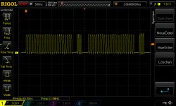
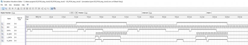
I attach the stopped clock logic and a scope shot I took from my Naim. It shows the stopped clock, taken from pin4@U6: it seems it is only stopped while the output of the DAC gets updated...
BTW the lower part of the original schematic around U51/U52 is a watchdog circuit because the PMD200 sometimes fails to be programmed - see here.
Attachments
Last edited:
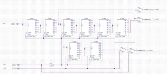
Stop-Clock2 20-Bit AD1862
@jpk73
I created it 😀
Stop-Clock2 - both channels are aligned together and with one stopped BCK moved for Left and Right DAC.
Latch (LRCK) is untouched 😎
At least 9 ICs are needed 🙂
@jpk73
I created it 😀
Stop-Clock2 - both channels are aligned together and with one stopped BCK moved for Left and Right DAC.
Latch (LRCK) is untouched 😎
At least 9 ICs are needed 🙂
Attachments
@jpk73
I created it 😀
Stop-Clock2 - both channels are aligned together and with one stopped BCK moved for Left and Right DAC.
Latch (LRCK) is untouched 😎
At least 9 ICs are needed 🙂
Fantastic!!!!!!!!!!!!!!!! 🙂🙂🙂
Stop-Clock2 - both channels are aligned together and with one stopped BCK moved for Left and Right DAC.
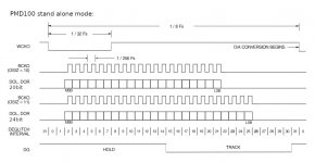
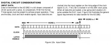
@miro1360, looking a bit closer at your diagram I think it might not work that way. From the PCM1702/4 datasheets: "if BCLK is stopped between input data words, the last 20/24 bits shifted in are not actually transferred from the serial register to the parallel DAC register until WCLK goes LOW. WCLK must remain LOW until after the first BCLK cycle of the next data word to insure proper DAC operation." This is also shown in the PMD100 datasheet, see this screen shot:
An inverted DG also might work as WCKO. Here is what I think how your digram could look like:
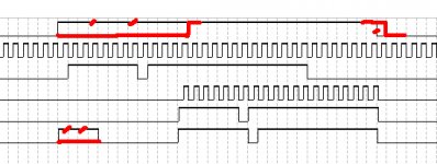
The timing diagram of the AD1862 shows the same requirement: WCKO stays low until after first BCK cycle of DATA transfer, goes high, and goes low again only after last BCK cycle of DATA transfer:
What do you think?
Attachments
Last edited:
The "unwanted" DATA is not feeded into the DAC because the clock is stopped. Making it total clean adds to the complexity 😀
PCM1702/4 is specific (because of the BCK requirement - the jitter in BCK can affect the sound), but the AD1862 has not this requirement and the output depends only on the low going LATCH (jitter in LATCH - LRCK can affect the sound) - That is why I don't want to modify the LRCK signal because the XMOS processor outputs it very clean 🙂
PCM1702/4 is specific (because of the BCK requirement - the jitter in BCK can affect the sound), but the AD1862 has not this requirement and the output depends only on the low going LATCH (jitter in LATCH - LRCK can affect the sound) - That is why I don't want to modify the LRCK signal because the XMOS processor outputs it very clean 🙂
@Hidy Seems like my DAC performs very good 😀
Fully agreed. Your dac not only measures well but also sounds amazing! It is my favourite dac now. Thank you miro for sharing the fruits of your labour with us. I solute you. You've brought joy to this world🙂

@jpk73 Yes it can be 🙂 That is how the first glue logic works.
@miro1360, I see! The first glue logic is beautiful as well, but the DAC at CLKout1 does not benefit from stopped clock in terms of pulse silence. Sorry for my persistence!
- Home
- Source & Line
- Digital Line Level
- DAC AD1862: Almost THT, I2S input, NOS, R-2R