ah : c10 & c19 printing is ok, my bad eyes, sorry !
a question please : why a voltage pin as close as the I2S pins ?No danger ?
a question please : why a voltage pin as close as the I2S pins ?No danger ?
@wealas
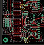
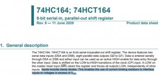
Don't install shift registers and feed chips directly (wires can be installed directly on SMD pads). #538
@diyiggy
Nice experimenting, so you finally took the solder gun 😀
There can be tons of improvements 🙂
It is voltage output pin, you can feed additional digital circuitry from it.
>>Could it be usefull to make a list of I2S streamers able of these 64 bits
>>So Xmos chips are proof ?
XMOS with good clock is perfect. A list can be created 😀 @nano35 is intensively testing the RPI, @RickRay tested a Toslink to I2S #1213
@wealas
Don't install shift registers and feed chips directly (wires can be installed directly on SMD pads). #538
Hi Miro,
I’ll throw in my 2 cent request, can you add a TH pad next to each shift register smd pad that corespondents to direct feeding signal from a JLSounds I2SoverUSB. Thanks 🙂
Hi Vunce, do you mean like this?
Hopefully the output of shift register can stay connected during the use of external pin 😕
edit: It can't be ... there must be a switch or break on the wire to disconnect it from shift register 😀
Hopefully the output of shift register can stay connected during the use of external pin 😕
edit: It can't be ... there must be a switch or break on the wire to disconnect it from shift register 😀
Attachments
Last edited:
Yes, hopefully you will be able to keep the shift registers soldered on the board and not disturb them, if you disable the power to the shift registers and then used the direct feed through hole pads, I think that should work?
A switch could be wired in series with the jumper provisions to interrupt power.
A switch could be wired in series with the jumper provisions to interrupt power.
Last edited:
What type of switch? Jumper?
Clamp diode can be our enemy. If the shift register is without power, clamp diode from the input can power it 😀
Clamp diode can be our enemy. If the shift register is without power, clamp diode from the input can power it 😀
Attachments
Last edited:
Maybe my 2 cents is turning into 10 cents, LOL!
Not as easy as I thought, soldering to the SMD pads looks like the best option.
Thanks for considering it though, Miro.

Not as easy as I thought, soldering to the SMD pads looks like the best option.
Thanks for considering it though, Miro.
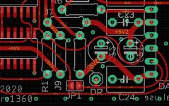
coming back on the 5V output pin : again is it not to close of the fragile Lrck input ???
I also think about the ground.
I also think about the ground.
I know we ask a lot and I'm thankfull for all the sharing here, but have you considered the same little board that is already fine, but with an opa 861 transimpedance stage for the I/V (no feedback, very few parts though smd are better for the caps but not always mandatory for stability depending on the powersupply quality and a further aop, double this time and I strongly think about an opa 1656 here (there smd and vias for decoupling being important imo for tweaking-adaptation taste purpose) ? While it coul be still be 627pb with two single pads !
What soft are you using please... I really should try to draw one... but the time...
now my main concern is about the lack of I2S uf-l just cause I'm lazy and also the jumpers between the dac chips and the front-end, mainly cause the soldering problems that are more harmfull that one believes imo.
What soft are you using please... I really should try to draw one... but the time...
now my main concern is about the lack of I2S uf-l just cause I'm lazy and also the jumpers between the dac chips and the front-end, mainly cause the soldering problems that are more harmfull that one believes imo.
Last edited:
>> is it not to close of the fragile Lrck input ???
Digital portion is not so sensitive 🙂
>> have you considered ......
I would like to see someone creating a similar replica of this DAC, but on his own path - Road 861
I used Autodesk Eagle ... such a hobby toy 😱
>> now my main concern is ....
"My recommendation: Start cheap and continue with improvements later." 😀
so no problem really with the ground of the close I2S ground and the one of the 5V ? Really ?
Pin 5 LRCK return path will follow its trace to DAC chips (the return path is the solid GND right under the trace).
Pin 6 GND is return path to an LRCK source.
... how do you see it?
Pin 6 GND is return path to an LRCK source.
... how do you see it?
hard to see with multiple layers design and bad eyes : so the two grounds (5V and I2S) are not shared close their gnd vias ? (it was what worried me but maybe it should not).
I remember also a Ti note about a neutral filer copper trace (not grounded) between two HF ground for avoiding lateral bouncing... while I don't know if it matters here. Example : Signal Ground Neutral then SGN then SGN in the illustration of an I2S signal (in fact to avoid lateral bouncing of two active lines on the same ground line. I assume a spacing to avoid that as well, hence my worry about seing a so close 5V signal & ground
I just should avoid two close such different grounded signals if it were sharing the same reference but it's certainly not tied on the same ground plane as you talk of underneath return path ?
It's also illustrate why I don't like 3D jumpers for HF signals (plus the soldering that is never good even on analog signals). Again 'm suspicious but perhaps it doesn't harm ?
Last edited:
It is voltage output pin, you can feed additional digital circuitry from it.
Whats the max current supported by this +5vdc output from the dac board? Can we use it to power another input dac board like coaxial/spdif to I2s output?
Thanks
this GND is enough ... maybe the simulation would show more 🙂 .. only a small flat solder joint can be forgiven in the HF
@manniraj I would say 500mA without harming anything
@manniraj I would say 500mA without harming anything
@manniraj I would say 500mA without harming anything
Wouldn’t the usable current be dictated by the psu powering the Dac board?
- Home
- Source & Line
- Digital Line Level
- DAC AD1862: Almost THT, I2S input, NOS, R-2R