Great, news, glad it's working well for you.
Doesn't pin 2 go to R3 and then to LRCLK on the DAC chip, though?
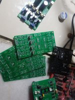
Despite fixing everything that one was still causing problems since I am not very patient when it comes to trouble shooting, making a new board is relatively easily thus threw that one away and made a new one.
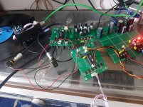
Now I have three working AD1865 (miro version) DACs. Next stage is testing it with different operational amp.
Have been building another version of AD1865 based upon Pavouk's work this one uses Vout instead of Iout, sine I still have 6 other AD1865 lying around may be will make them as well.
Any suggestions for casing, my initial idea was to throw away the DAC section of "Rod Rain DAC" the DAC section is ES9038Q2M, use the casing and amanero board but this PCB (miro's) is wider so have to find some other casing.
Attachments
@rehanabid Glad to see your progress 
... the case selection depends on the final DAC size 😎
DIY chassis are on audiophonics.fr 😉
Navigate here: Home>DIY enclosures and cases
... or aliexpress, ebay 😀
... the case selection depends on the final DAC size 😎
DIY chassis are on audiophonics.fr 😉
Navigate here: Home>DIY enclosures and cases
... or aliexpress, ebay 😀
Thanks @miro1360, audiophonics has a good collection of casings.
My idea is to add amanero, may be in the later stages an SPDIF interface, a LCD/OLED (though I still have a couple of old VFD_HD44780 compatible but they are power hogs) to display track bitrate, flac or DSD,a mcu for input selection USB/SPDIF etc.
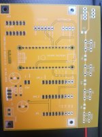
Made this modular controller board a while ago around arduino it has all the necessary I/O I think I'll use it as well.
My idea is to add amanero, may be in the later stages an SPDIF interface, a LCD/OLED (though I still have a couple of old VFD_HD44780 compatible but they are power hogs) to display track bitrate, flac or DSD,a mcu for input selection USB/SPDIF etc.
Made this modular controller board a while ago around arduino it has all the necessary I/O I think I'll use it as well.
Attachments
@Sergelisses
PCBs are often ordered from jlcpcb (during checkout select europacket, it is best shipping/price for the EU, or fedex). Alternatively, you can use some local service, but the price will be hardly competitive. See the price for 5pcs including good shipping in the EU.
Sorry I picked up a very old post but for the benefit of DIYers my experience is as follows:
1)PCBWay excellent tracking of project progress, if you share your project on their forum and if the PCBs are ordered by other DIYers you get a share of the money, normally I have over $20 credit there due to sharing. Downside is that their solder mask is not up to the mark and it has bubbles many a times. Since my credit card is from Zone B therefore I have to pay them through AliExpress.
2)JLCPcb excellent tracking during processing and after dispatch, I have no idea about project sharing, PCB quality is excellent so is customer service, down side is their preferred shipping method of SF Express which to my bitter experience are fraudsters. Payment is easy.
3)SeeedStudio poor tracking during processing, after dispatch excellent tracking price is the same as above two but PCB quality is absolutely fantastic. They offer so many discount coupons that after a couple of projects you can get one absolutely free (excluding shipping of course). Payment is easy can pay through credit card or debit card.
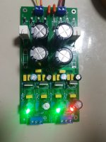
@miro1360 PCBs for PSU arrived on Friday evening and I decided to populate couple of them started with one, since I am using AD1865 thus changed the value of resistors on 12 volt rails for 5 volts.
However I am running into a problem one of the rails the positive side analogue supply side, when I switch on the PSU the voltage at positive analogue rail starts off at +5.05 volts then it starts dropping off and stabilizes between 1.96 to 2.02 volts that's when the LED turns off as evident in the pictures and video.
Frankly I have never used LT1963/3015 combination, always preferred using 317/337 combo, I have no idea whether the problem is with LT1963 or something else I have removed the trim pot and the optional resistor, after a few tries fixed the R2/R1 combo at 1.18K and 330 ohm but this weird problem is prohibiting me from using this PSU.
Any ideas/suggestions will be appreciated.
Attachments
You may want to check on the fixed resistors mod, mine power up fine with the trimmer, all output voltages very stable.
@rehanabid What is the exact part number of yours LT1963 regulator? There are different types. Besides the adjustable used in this project there exists fixed voltage versions.
584-LT1963AET#PBF is adjustable
584-LT1963AET#PBF is adjustable
I purchased it from AliExpress the part No# LT1963EQ its a TO263 packing and not TO220, I had to improvise to put it in the pcb.
One LT1963 is giving a fixed output of 5.05 volts with the trim-pot or experiment with R2/R1 combo it gave me a range of 3.8 to 8.6 volts on the rail, but the other one is just behaving strange, I don't know whether I have to replace all the capacitors on the rail, check diodes or tray and replace the regulator, what I am curious is about the odd behavior of the LDO.
BTW I am using a toroid of 6+6 volts with the bridge rectification minus forward biasing compensation the voltages are around (8.3 - 8.6 volts)
Last edited:
Check the marking on the LT1963 if they are the same.
Or it may be a damaged regulator, aliexpress risk 🙂
Or it may be a damaged regulator, aliexpress risk 🙂
@rehanabid What is the exact part number of yours LT1963 regulator? There are different types. Besides the adjustable used in this project there exists fixed voltage versions.
584-LT1963AET#PBF is adjustable
I made this mistake, it took some head scratching to figure out why the voltage was wrong and didn't change with any adjustment...
Hi,
Is there a difference on the new uf-l v1.3 board between the I2S inputs of the 4X2 pins header and their pcb marking description writting on it, please ?
Do we have a difference between Bck, Lr and Data VS the previous no uf-l board ?
I think I fried my JLSOUNDS v3 because of a bad reg that outputed 9V instead the 5V needed !
I hate the diy wires for pin header connector and the screwable conector on power supply that don't allow easy double wirering, uh !
@diyiggy
There is no difference, all pins are digital inputs only 🙂 The uf-l v1.3 I2S connector is all gnd with 3 digital inputs (the marking is correct).
Pin 7 on some previous PCBs is +5V output, not the uf-l.
Why the reg outputed 9V instead of 5V? 😱
What is a reason to use the hated connectors? 😕
Are there no pluggable connectors with the 5.08mm raster? Just stay a happy DIYer and use your favorite parts ... you did it in the past
Miro,
I don't know why, that's a programable reg I used in a further version that has a problem I didn't see before despite the resistor values are good. It's a classic TSA7 board and on 5 I use, just this one had a problem despite the good resistors values that set the V output !
I want to use a uf-l board I made to add the header and the divider to debug and make some tests with the JLSOUNDS board. I just saw it was not the same order for the I2S than the previous board you made, hence the question.
The previous board had the ideal order for the JLSounds but the Gnd as it's on a second row on the JLSOUNDS and on the same raw in the AD1862 board. On the newest there is two rows with the ideal Gnd on the second row as the JLSOUNDS board to use a female header than JLSOUNDS provides. Unfornatully the order of the I2S is not anymore in the same order than the previous AD1862 board. So I asked just in case it was a printing issue as I remember a member asked about the order when you gave the gerbers !
That's just me, I hate the little wires with bad diy isolation because of shorts, etc. Just because I do many tests about supplys, passive parts, etc ! So I use most often uf-l pr solid headers and not individual wires that are a nightmare, at least for me !
Yes, no luck about the bad regulator ! WHatever I knew already the lesson : always check power supplies before to fire up !
Unfornatully, being not at my main location, I have no I2S else board to check...
Btw I like the uf-l version: uf-l pads direct to the AD1862, the little uf-l pads giving by themselves enough attenuation often and the I2S boards having all resistors in serie at the outputs.
There are also more room for the caps and the I/V resistor. While the 0,1 uF seems farer from the pins : anyway here I don't use 5 mm MKT but smd caps from CDE I solder with flux between the vias ! But here in my question I want to use for debug the 4X2 header.
Anyway, I asked to JLSounds what happen with a higher voltage applied on the H3 connector... I assume the reg fired only I hope or it's direct for the bin and at close to 120 euros the board with the shippment, that's sad !
The front-end connection is a real problem when it comes to test several main boards with one front-end !
Last edited:
Rehanabid;
On the LT1963 remove C17 - goes from adjust pin to output I think going from your pcb pic.
The LT1963 is different to the LT3015 and does not like to see any capacitance across this adj resistor.
The LT3015 is different & adding a capacitor across that adjust resistor reduces noise.
I got caught out the same way & wrongly assumed the LT1963 was the same.
Recheck the LT1963 data sheet & you will see there is no mention of a capacitor across the adjust resistors.
Cheers
Clay
Rehanabid;
On the LT1963 remove C17 - goes from adjust pin to output I think going from your pcb pic.
The LT1963 is different to the LT3015 and does not like to see any capacitance across this adj resistor.
The LT3015 is different & adding a capacitor across that adjust resistor reduces noise.
I got caught out the same way & wrongly assumed the LT1963 was the same.
Recheck the LT1963 data sheet & you will see there is no mention of a capacitor across the adjust resistors.
Cheers
Clay
The interesting thing about this C bypass is that in the non-adjust version (1.2V) adj pin is joined internally to OP.
There is likely some lowish value resistor that can be inserted at Adj pin whereby allowing stability with bypass C. The problem with not bypassing
(R2 on data sheet) is the noise multiplication. This can clearly be seen on P9 data sheet, even at 3.3V OP the noise is more than doubled. If you use the
reg for say 15V, there will be a huge noise multiplication at OP.
TCD
Hi Terry - nice to hear from you.
Hey just wondering if we are looking at the same data sheet for the LT1963.
I have rechecked & I can find no reference to a CFF (feed forward capacitance) across R2 anywhere.
With the LT3015 yes CFF is referred to a lot & certainly drops the output noise by a significant amount.
Hey just wondering if we are looking at the same data sheet for the LT1963.
I have rechecked & I can find no reference to a CFF (feed forward capacitance) across R2 anywhere.
With the LT3015 yes CFF is referred to a lot & certainly drops the output noise by a significant amount.
Subscribed!
If PCBs will be available I will take some of them.
Very promissing thread!
PCBs are available to order directly from a prefered manufacturer (gerber files are for download) ... #2180
...
Yes, no luck about the bad regulator ! WHatever I knew already the lesson : always check power supplies before to fire up !
...
Few days ago I reversed the polarity and fried all ukz capacitors along with THS4031 opamps 😀😀
@meanie , @miro1360, @diyiggy, @clay-speakers , @terry demol
Thank you all for your suggestions and inputs since I am out of town will share my further findings on this next week (having almost 5 holidays in it).
I have given consideration to all your suggestions part of my professional life to remove all doubtful variables and try and come to a conclusion with highest probability so here goes:
1) all LT1963 are from the same batch it means if one LT1963 is providing a stable output of 5 volts then the other should also.
2) Capacitor same issue it is true for both LT193 one should not be behaving differently from the other.
3) resistor mismatch
4) Problem at the diode level
5) faulty large capacitors
6) problem in the PCB
I think I have pretty much ruled out first two but will explore rest of the 4 possibilities, hopefully will be able to populate the other PCB for comparison.
My only unsolved question is why the output starts at 5 volts and then drops to stabilize between 1.96 to 2.xx volts.
- Home
- Source & Line
- Digital Line Level
- DAC AD1862: Almost THT, I2S input, NOS, R-2R