...(near) -200dB @ 1.4V input
Hi Frans
This seems suspiciously excellent.
I have seen other suspiciously excellent simulations that were unrealistic because of the use of the NMOS/PMOS Spice model.
I notice you use it too but unfortunately it does not model capacitance modulation correctly, the VDMOS model would probably be far more accurate.
There is a thread on this in the software and tools forum.
Best wishes
David
...And thanks for the welcome to the diyAudio community.
My pleasure.
Frans' (FdW) post #18 and my reply #21 reminded me of one of the reasons why I looked forward to have your input.
I had a few questions about the work you and Keantoken did on VDMOS models, it starts >here<.
Perhaps you could read and comment?
Best wishes
David
Hi Frans
This seems suspiciously excellent.
I have seen other suspiciously excellent simulations that were unrealistic because of the use of the NMOS/PMOS Spice model.
I notice you use it too but unfortunately it does not model capacitance modulation correctly, the VDMOS model would probably be far more accurate.
There is a thread on this in the software and tools forum.
Best wishes
David
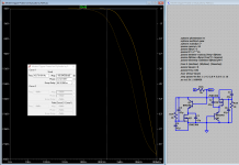
I know 🙂 but who cares, the thing is build and functions, sound wise it is real good, the fact is @ -3dB it being -140 or -200dB does not make a differences. What the simulation shows is a [extremely] viable and simple clipper, with [almost] no effect on the signal (as long as it not operates) because it is a shunt. In practical implementation I have lowered the series resistor to 220 Ohm, this will improve the 'responsiveness' of the clipper and lowers any possible distortion introduced by the clipper, but it will form a larger load (when clipping) on the source.
In addition to the above; most of the nasty's (if any, and when any) are hidden behind the transdiodes formed by the BFR540's.
When I add (worst than) worst case capacitors to the schema, 47p Cgs, 47p Cdg and 47p Cds, and then run a frequency analysis, it shows the -100mdB at 185kHz any nasty's produced by the MosFet and conveyed through these capacities must IMHO be of no real interest.
The model is surely not complete, and it would be interesting to see this simulation done with better models (but I do not have them, and I can not [am not able to 🙂] make them). But all documentation on MosFet behavior seem to tell me that there wil be no real ugly problems.
Using a smaller series resistor(R16 1k in the simulation) will lower the influence of the capacitive behavior of the circuit, mostly by lowering the source resistance, and drive the MosFet [even] more in saturation, this should not have a negative influence [I do think it will be positive] on the clipper (Analog Design Essentials page 17/18 0131/0132 etc)
In real life, I (and other listeners) have not been able to hear the clipper being engaged and/or disengaged while playing at loud [but non clipping] levels (but that is subjective 🙂)
Attachments
Last edited:
Running the sim with this model
*VDMOS with subthreshold (c) Ian Hegglun Aug 2015
.model IRF640-75C VDMOS (Rg=5 Vto={4.30-6m*50} Lambda=3m
+ Rs={35m*(1+3.5m*50)} Kp={13.0/(1+8.8m*50)}
+ Ksubthres={0.23*(1+4m*50)} Mtriode={0.35} Rd={0.1*(1+5m*50)}
+ Cgdmax=2600p Cgdmin=10p a=0.35 Cgs=1250p Cjo=3000p
+ m=0.75 VJ=5 IS=1n N=1.3 Rb=0.01 )
gives about -65dB(THD) but it is not fair to compare a small signal MosFet with this power device.
Concluding, I have no good model(s) and/or idea(s) to improve the sim
Last edited:
My pleasure.
...
I had a few questions about the work you and Keantoken did on VDMOS models, it starts >here<. Perhaps you could read and comment?
David
Thanks for you interest and I'd like to help.
I'll PM you on where we can go from here since this thread was not intended for discussing VDMOS model details.
Ian Hegglun
Dear Mooly!
Please check my file,
however the results are similar like yours.
Sorry to push in. But one problem. Did you notice there are 100 ohm base-emitter resistors added (R7,R8) to the power transistors that Win's original circuit did not have?
The attached circuit has them removed back to original and the bias reset back to 100mA.
THD falls only slightly -- it's still not the 0.01% that Win's Figure 11 shows.
But this is probably due to different Beta's in the drivers and power transistors. If you match the beta's of upper and lower halves you should be able to remove most of the second harmonic, so the THD gets closer to Wim's 0.01%.
Then see if you can get Wim's THD at 20kHz.
Ian Hegglun
Attachments
Thanks for you interest and I'd like to help.
I'll PM you...
Or reply in the linked VDMOS thread itself? That way the questions and answers are all in the one place.
Also means I don't have to clean out my DIYaudio mailbox, which is full at the moment😉
Best wishes
David
... BiModal-4v1-CSD....
Dear Ian!
You wrote in LAv13 that the pcbs for the amp will be avaliable when one will order LAv8.
What if I already have LAv8?
Do you provide the other way to order the pcbs version 4.1?
Running the sim with this model
*VDMOS with subthreshold (c) Ian Hegglun Aug 2015
.model IRF640-75C VDMOS (Rg=5 Vto={4.30-6m*50} Lambda=3m
+ Rs={35m*(1+3.5m*50)} Kp={13.0/(1+8.8m*50)}
+ Ksubthres={0.23*(1+4m*50)} Mtriode={0.35} Rd={0.1*(1+5m*50)}
+ Cgdmax=2600p Cgdmin=10p a=0.35 Cgs=1250p Cjo=3000p
+ m=0.75 VJ=5 IS=1n N=1.3 Rb=0.01 )
gives about -65dB(THD) but it is not fair to compare a small signal MosFet with this power device.
Concluding, I have no good model(s) and/or idea(s) to improve the sim
One last word about this [from me], I do not use simulations to 'specify' my circuits, to 'measure' my circuits or to 'predict behavior' of my circuits, I do use simulations to see if 'it' may work, and then I use measurements to see how 'it' is working and how 'it' might be improved.
One last word about this [from me], I do not use simulations to 'specify' my circuits, to 'measure' my circuits or to 'predict behavior' of my circuits, I do use simulations to see if 'it' may work, and then I use measurements to see how 'it' is working and how 'it' might be improved.
Same here. I use it for 'proof of principle' and then move into actual hardware.
Jan
...I do use simulations to see if 'it' may work, and then I use measurements to see...
OK, I am interested to see the measurements of the distortion too.
What did it measure?
Best wishes
David
OK, I am interested to see the measurements of the distortion too.
What did it measure?
Best wishes
David
This is going in a direction that I do not like to follow, this is also why I never publish in an 'public-mail-forum' environment (and I do have more that 40 years experience with this). It was the question from Ian that lured me to publish 🙂
Measurements where done with my QA401 and on the basis of these measurements it was decided to test/try/audition and then add the circuit to my amplifier product. It also was decided that the usage of the clipper must be selectable, so I did add a switch.
What the exact results where of the measurements, now more that 2 years ago, I do not know. Better than -90dB THD or I would not have decided to use the clipper in the product. Listening test must also have been positive (for the same reason).
Why not build the circuit and try for your self, it is only [I guess, about] 3$ or so of components.
To be clear, for me (and my listening panel) the addition of a circuit (like this) would be acceptable if (at moderate to loud levels) it was (near) undetectable to the ear, and when at extreme levels there would be a positive improvement compared to not including it (as long as it is selectable [to use or not to use])
Last edited:
... this is also why I never publish in an 'public-mail-forum' environment ...
Please replace 'never' with 'almost not' 🙂
Anyone interested in the new VDMOS subcircuit models being developed by Keantoken and myself - then see my post hereOr reply in the linked VDMOS thread itself?
As I mentioned earlier in this thread that you can view the new quasisaturation VDMOS subcircuit working in my simulation file for the 'Bimodal 4v1 CSD...' zip on my web drive. And there's the new electrothermal VDMOS subcircuit working in my simulation circuit 'idrive' zip now on my web drive (link in my profile then go to the 'diyAudio' directory).
All these new subcircuits need documentation before they will be officially released for all to use. No promises when that will be.
Last edited:
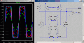
Yet another soft-clipper idea I came up with just yesterday. THD@20kHz 3dB below visible clipping isn't super low (still good enough for my needs) but my goals were different: low cost standard parts, adjustable "hard" ceiling but still with round edges, and a 5% ceiling accuracy without selection or trimming and from 20°C to 70°C ambient.
Not built yet so I don't know how close I'll actually get.
Not built yet so I don't know how close I'll actually get.
Attachments
I'm sure this will be clear as mud, but here it goes.
In an op-amp, the input stage drives the rest of the amp. Any distortion in the required drive current shows up as distortion at the output. Whether your output BJTs are driven by collectors or emitters, the base drive current they require is exactly the same for a given output, same harmonics and everything. And unless you have something parasitically shunting the voltage follower stages (Miller compensation, Early effect, bootstrap), converting output drive voltage into VAS current harmonics, then the drive current which the LTP must supply also contains no difference in harmonics. And so no difference in distortion at the output of the amp, assuming that the feedback point is at the output and not shared with other points (VAS to feedback miller cap for example).
Also think of it this way. An emitter follower or source follower output stage cannot be current-driven at audio frequencies, if it is in a feedback loop. If you think otherwise, use an AC current source to inject current into the OPS base nodes and see what the actual impedance is there at audio frequencies. It will be extremely low unless your have a weak feedback loop. This is because any current going in or out of the OPS bases is treated as an error signal and removed by the preceeding stages as they are driven by the input stage, so that it doesn't change the output voltage from where the input stage is told it should be.
That is not a refutation of Ian's work. But I think "collector driven output transistors" would be less onerous as a working description of the ideas here. This is for the same reason I think "emitter feedback" would be much more sober a term than "current feedback".
There is a sort of infectious mathematical idealism that leads to the black-and-white thinking of current drive vs voltage drive, current sources vs voltage sources, etc. Well, transistors are 3-or-more terminal devices and the currents and voltages between those pins have mixed relationships. That is why Satan invented S-parameters, as a way to analyze them all in the most brutal, clinical, and impenetrable way.
Anyway, I just realized Ian never made any claims about reducing crossover distortion. So my comments are really moot. Let what follows be a refutation in case anyone else thinks so.
With collector-driven BJT outputs, the advantage Ian seems to be using is to drive the bases independently. Otherwise you always get the same crossover shape caused by exponential (Vbe) transfer curves in anti-parallel. This can be done with emitter-drive as well, but collector-drive has the advantage of simplicity and that the distorted Vbe waveforms are not carried any further into preceeding stages as they would be with emitter drive.
The new arrangement makes the crossover distortion harder to probe, but that doesn't mean it isn't still there. Add the Vbe waveforms of the BJT outputs and there it will be. Independent collector driven output BJTs will not have the exact same transverse (collector-to-collector) current waveform, but there is nothing here that will explicitly quarantine or remove the Vbe waveforms any more than the Early voltage of the drivers will allow.
But let's say that the collectors driving the output BJTs have infinite Early voltage. Look at Figure 3 in Ian's article, assuming Hfe=100 for the transistors. Roughly, Ib(Q4)=Ie(Q4)/100. Ic(Q1)=Ib(Q4), so Ic(Q4)=Ic(Q1)*100. For all intents and purposes, Q1 and Q4 are the same transistor. And this transistor has an emitter resistor - R1. In fact, Q1 and Q2 look a lot like a standard EF output stage. If we make R1 and R2 22R, then the whole arrangement behaves like a standard EF output stage with 0.22R resistors, with the exception that the input is referenced to ground and the output current has been moved to a separate node. Thermal behavior is different of course, but there is nothing here that actually has the ability to change the crossover function.
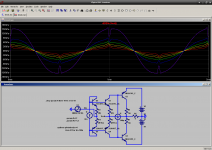
For visual appeal, I've attached an image of a simulation I did with a similar output stage, sweeping the driver emitter resistor value. The lower drivers have higher emitter resistors to account for the PNP output having extra gain.
There is a sort of infectious mathematical idealism that leads to the black-and-white thinking of current drive vs voltage drive, current sources vs voltage sources, etc. Well, transistors are 3-or-more terminal devices and the currents and voltages between those pins have mixed relationships. That is why Satan invented S-parameters, as a way to analyze them all in the most brutal, clinical, and impenetrable way.
Anyway, I just realized Ian never made any claims about reducing crossover distortion. So my comments are really moot. Let what follows be a refutation in case anyone else thinks so.
With collector-driven BJT outputs, the advantage Ian seems to be using is to drive the bases independently. Otherwise you always get the same crossover shape caused by exponential (Vbe) transfer curves in anti-parallel. This can be done with emitter-drive as well, but collector-drive has the advantage of simplicity and that the distorted Vbe waveforms are not carried any further into preceeding stages as they would be with emitter drive.
The new arrangement makes the crossover distortion harder to probe, but that doesn't mean it isn't still there. Add the Vbe waveforms of the BJT outputs and there it will be. Independent collector driven output BJTs will not have the exact same transverse (collector-to-collector) current waveform, but there is nothing here that will explicitly quarantine or remove the Vbe waveforms any more than the Early voltage of the drivers will allow.
But let's say that the collectors driving the output BJTs have infinite Early voltage. Look at Figure 3 in Ian's article, assuming Hfe=100 for the transistors. Roughly, Ib(Q4)=Ie(Q4)/100. Ic(Q1)=Ib(Q4), so Ic(Q4)=Ic(Q1)*100. For all intents and purposes, Q1 and Q4 are the same transistor. And this transistor has an emitter resistor - R1. In fact, Q1 and Q2 look a lot like a standard EF output stage. If we make R1 and R2 22R, then the whole arrangement behaves like a standard EF output stage with 0.22R resistors, with the exception that the input is referenced to ground and the output current has been moved to a separate node. Thermal behavior is different of course, but there is nothing here that actually has the ability to change the crossover function.
For visual appeal, I've attached an image of a simulation I did with a similar output stage, sweeping the driver emitter resistor value. The lower drivers have higher emitter resistors to account for the PNP output having extra gain.
Attachments
Last edited:
Did you notice Wim de Jagger is using the term "power transistors driven by a current source" Post #15... But I think "collector driven output transistors" would be less onerous as a working description of the ideas here.
Your preceding post (and this one) seem to be related to the issue of whether you still have current driven power transistors once you apply some loop feedback such as via the driver transistors.
I think it is a similar thing when you apply voltage feedback around a transconductance opamp. Does the voltage feedback suddenly make the transconductance opamp a voltage opamp? To the outside world you now have a voltage amplifier with a low output resistance -- but we still have a transconductance opamp plugged into in that circuit, do we not?
If you run the circuit open loop, which in your stimulation means breaking the feedback link from R6,7 to R1,2 and then connect R1,2 node to COM (and reduce the input level). BTW I like you simulation plots.
Current driven power transistors is not a way to reduce crossover distortion. Current driven power transistors makes more crossover distortion than voltage driven power transistors because of low current Beta fall and high current Beta fall. The low current Beta fall can be mitigated by adding the base current source (seen in your circuit) and the high current Beta fall is mitigated (best we can) using modern RET power transistors (which have high IKF model parameters well in excess of the output current).
Although we get slightly higher crossover distortion we can now maintain the optimum bias. Also with current driven power transistors you don't need emitter resistors in the power transistors - less board area and less wasted power. And you can parallel power transistors without current hogging. That's what I found in my amp in Linear Audio Vol.13.
But there's still a cross-conduction problem to solve, where distortion rises heaps at 20kHz. And you get lots of heat generated no load with full output swing at 20kHz.
See if you simulation shows higher distortion at 20kHz. And what's the dissipation rise to with no load and full output swing at 20kHz?
Last edited:
- Status
- Not open for further replies.
- Home
- Amplifiers
- Solid State
- Current-Source-Driven-power-transistors-and-mitigating-cross-conduction-distortion