I have considered making the very same argument. The input stage does not experience a difference between the two circuits. And now, we no longer have to deal with the argument that the input stage current flows only through Rg. Now the input stage current flows from the "new" output, Vth.
But the same current flowing from the output through the input stage will, I fear, still be ignored in favor of the observation that the transconductive portion of the input transistor current is a function of by vb - ve. For a few folks, for some reason, this excludes the possibility of any kind of feedback of any current. It is this assertion that needs to be at the forefront of further discussion between the two camps. But perhaps Hierfi's Thevenin equivalence will move us closer.
I expected you to be the first to see things into this translation Chris.
I think the problem is that when I write :
"Single input device CFA don't have COD behaviour."
Your reply is :
"But an (otherwise suboptimal) shunt compensation in a sigle ended CFA will show the COD effect. "
So instead of giving your very good advices on symetrical slewing, try to read slowly.
I have to agree with Syn08. I really don't know what you are trying to show here. As mentioned many times before, you argue over where we know there is an overlap in behaviour (so what?) and/or with sub-optimal circuits and the result is we just go around.
I will step out of this discussion for a while.
...(from an earlier post)
This needs more study, there are multiple issues in looking at this in all detail. Characteristic curves can be vs. Vbe or Ib, since beta can be a strong function of Ib I personally find this approach (bipolars as current controlled devices) virtually useless. My last product with patent was a constant BW log amp where the log conformance of a tiny short base NPN was quite good from 100fA to 100uA (collector current).
Scott, I'm not arguing for the general usefulness of such measurements, just that for a constant ib, partial ic w.r.t. vce seems pretty constant as the DC value of vce is varied.
Scott and Ian, I intend to measure ic/vce with constant ib on a number of 2N3904's I have. I'll repeat with constant vbe and with Ie set to 1mA. It'll be nice to check this against the two versions of models in LTSpice that Ian discussed. Any suggestions/comments regarding such a test?
I expected you to be the first to see things into this translation Chris.
You know me well already, my friend.
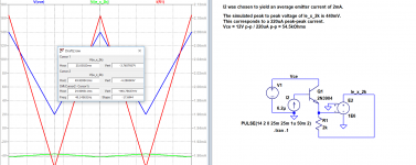
Below is a Thevenin translation of a simplistic Rf - Rg feedback network. This represents the foundation of the thought process behind several arguments presented in the past.
It is considered that much of the difficulty in comprehending the nature of a CFA results from the elusive relationship that the In- terminal has to an elusive voltage that must exist to support the functionality of the device. The Thevenin translation is intended to identify that elusive potential as V Thevenin.
Using the Thevenin translation it can easily determine the value of Vin necessary from selecting an arbitrary Vout, and specifying resistances at the Tz node and for Rf and Rg. These Vout and Vin values can then be applied to the simplistic non-translated Rf - Rg network to verify the summation of currents at the In- terminal and their current phase relationship.
Before presenting any further arguments, does anyone consider such translation as potentially useful to simplify their the understanding of a CFA.
As no one disputed your translation, I guess everyone agrees with.
So I have to congratulate you as you demonstrate the assertion from Forr :
A CFA is an Unbuffered VFA.
Doing the same test as with the BC550 in #2119, I got Ro=196K @ Ie=1mA for the 2N3904 with LTSpice.Scott and Ian, I intend to measure ic/vce with constant ib on a number of 2N3904's I have. I'll repeat with constant vbe and with Ie set to 1mA. It'll be nice to check this against the two versions of models in LTSpice that Ian discussed. Any suggestions/comments regarding such a test?
Hans
Scott and Ian, I intend to measure ic/vce with constant ib on a number of 2N3904's I have. I'll repeat with constant vbe and with Ie set to 1mA. It'll be nice to check this against the two versions of models in LTSpice that Ian discussed. Any suggestions/comments regarding such a test?
Resolving the differences might be difficult. The point was when you force base current Vce modulation will change Vbe and forcing Vbe the Ib is what changes.
As no one disputed your translation, I guess everyone agrees with.
So I have to congratulate you as you demonstrate the assertion from Forr :
A CFA is an Unbuffered VFA.
A lack of response never supports a conclusion of agreement Herve.
The Thevenin translation is of a basic form that doesn't yet include the significance of the internal Ro of the In- terminal, being in series with the translation. This Ro isn't a real Ro, rather a function of some equivalency of a transistor operating at some current, as I perceive being the object of discussions currently taking place.
The determination of a CFA being a CFA or VFA is considered, in my thinking, dependant upon the value of R Thevenin (Rf and Rg in parallel) in relation to the Ro as seen into the In- terminal. It is unclear if there exists any alignment with the results using Middlebrook, although it too is looking into the In- input.
A CFA is an Unbuffered VFA.
So then, if I take the buffer off of a VFA I end up with a CFA?
That doesn't seem very useful in trying to decide whether a circuit is a VFA or a CFA; you just shifted the problem to the problem of defining 'what is a buffer' or 'what is a VFA' in this context.
'A VFA is a buffered CFA' is just circular.
Jan
Last edited:
Which was first stated in post #60 more than a year ago in this thread, albeit in the reverse notion of a VFA being a buffered CFA.So I have to congratulate you as you demonstrate the assertion from Forr :
A CFA is an Unbuffered VFA.
Happy New Year!
EDIT: What's a CFA then? To me, an OpAmp-type closed-loop circuit whose open-loop gain is *not* independent of the network impedance presented on the (-)-input pin, actually OLG scales well with network transconductunce over a reasonably wide range. This happens to lead to the first-order independance of BW vs gain with the standard Rf, Rg gain network, with Rg varied.
Last edited:
A lack of response never supports a conclusion of agreement Herve.
A french proverb says the contrary : "Qui ne dit mot consent."
The Thevenin translation is of a basic form that doesn't yet include the significance of the internal Ro of the In- terminal, being in series with the translation. This Ro isn't a real Ro, rather a function of some equivalency of a transistor operating at some current, as I perceive being the object of discussions currently taking place.
The determination of a CFA being a CFA or VFA is considered, in my thinking, dependant upon the value of R Thevenin (Rf and Rg in parallel) in relation to the Ro as seen into the In- terminal.
What is Ro ? Zin- ?
Which was first stated in post #60 more than a year ago in this thread, albeit in the reverse notion of a VFA being a buffered CFA.
Happy New Year!
EDIT: What's a CFA then? To me, an OpAmp-type closed-loop circuit whose open-loop gain is *not* independent of the network impedance presented on the (-)-input pin, actually OLG scales well with network transconductunce over a reasonably wide range. This happens to lead to the first-order independance of BW vs gain with the standard Rf, Rg gain network, with Rg varied.
I give back to you the definition which I completely agree.
Happy new year to every one !
A lack of response never supports a conclusion of agreement Herve.
The determination of a CFA being a CFA or VFA is considered, in my thinking, dependant upon the value of R Thevenin (Rf and Rg in parallel) in relation to the Ro as seen into the In- terminal. It is unclear if there exists any alignment with the results using Middlebrook, although it too is looking into the In- input.
My opinion is that we should distinguish between CFA and VFA (which I prefer to use to denote topologies), and current and voltage feedback (c.f and v.f.), which can be measured by MDIT.
In a CFA topology, input stage signal current flows through the feedback network (which in some cases can do double duty as a bias network.) In a VFA, this doesn't happen. Of course, composite designs with two different types of feedback can exist. If these come into wide use, it might make sense to assign a separate name to such.
It can be shown that at adequately high loop gains, if Rf || Rg > Z(in -), c.f. predominates. Otherwise, v.f. does. Of course, the application of MDIT has the final say.
I was curious about the internal behaviour when CFA's is in invertingn closed loop configuration, alos said "virtual ground". I have never seen this scheme used for CFA's but it seems to work as. intended with the inverting input being very close to the ground potential.
The first circuit has it gain set by the negative feedback divider Rfi/Rgi.
The second one is a transimpedance circuit, its output voltage being equal to the voltage across feedback resistor Rft due to current Igt.
Current Ie and voltage Vbe of input transistor T1 have very stable values for variations of Rg from 2 Ohm up to 20 kOhm.
An externally hosted image should be here but it was not working when we last tested it.
An externally hosted image should be here but it was not working when we last tested it.
Last edited:
EDIT: What's a CFA then? To me, an OpAmp-type closed-loop circuit whose open-loop gain is *not* independent of the network impedance presented on the (-)-input pin, actually OLG scales well with network transconductunce over a reasonably wide range. This happens to lead to the first-order independance of BW vs gain with the standard Rf, Rg gain network, with Rg varied.
Bingo!
Note: not any dependences of the OLG on the feedback network will provide the CFA small signal properties, it would be more correct to state that in a CFA the Loop Gain depends on the feedback resistor only (and not on the noise gain as in a VFA).
Last edited:
The smilies on this forum have been the same for donkeys' years and are rather a mixed bag with notable omissions. I just can't find the right one. Instead, here's something seasonalYes, it belongs with first cycle distortion.

I was curious about the internal behaviour when CFA's is in invertingn closed loop configuration, alos said "virtual ground". I have never seen this scheme used for CFA's but it seems to work as. intended with the inverting input being very close to the ground potential.
It's appeared on every data sheet for years and I suggested a while ago it makes things clearer. Maybe you have missed some other things?
I've made lots of use of this with the AD844. Like with any honest CFA, current at -in = output current at Tz. So you can set voltage gain by the ratio of series R at -in to load R at Tz.
Jan
Jan
This needs more study, there are multiple issues in looking at this in all detail. Characteristic curves can be vs. Vbe or Ib, since beta can be a strong function of Ib I personally find this approach (bipolars as current controlled devices) virtually useless. My last product with patent was a constant BW log amp where the log conformance of a tiny short base NPN was quite good from 100fA to 100uA (collector current).
Hi Chris, all,
I think there is an anomaly created by the Gummel Poon BJT model used in SPICE...
...Thanks, CPaul, for raising it; it looks like we now have a good reason to convert to the VBIC model.
I would be surprised if the current LTSpice models would be so wrong.
Hans
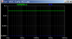
As threatened 🙂 I measured the Early resistance ro of a 2N3904 at Ie = 2mA on the bench and compared it to that predicted by an LTSpice sim. The results differed by a factor of 2.5 (134k measured vs. 54.5k simulated.)
I don't know the variations of ro from transistor to transistor, but this seems reasonably close. It would appear to be a confirmation of the sim I did showing the CFA gm and ro input transistor current contributions becoming almost equal at high at loop gains. I question whether it justifies disposing of the Gummel Poon models in favor of the VBIC versions, but I'd be interested in others' comments.
Attachments

VBIC update
The anomaly I found in the GP model was specifically the ratio of Ic6/Vbe. When the Tz termination resistance was varied in your test circuit (Post 1872 AD844) Current Feedback Amplifiers, not only a semantic problem? you found a massive unexpected drop from 38mS to 0.15mS!! when this should not change much at all.because you are only altering the termination resistance of the output of the current mirrors and there should be negligible change in the DC bias.
I don't see how just measuring the Early effect resistance 'ro' relates to this anomaly. I think you would need to make the circuit you simulated and bench test it to find the ratio of Ic/Vbe for Q6 with AC signals.
As I demonstrated with the VBIC model in your circuit the ratio of Ic to Vbe was quite close to the expected constant gm value of 30-40mA/V at 1mA. and that over the wide range of Tz loading resistances.
I have since found the VBIC's small spread is mainly determined by the choice of parameter 'mc' which is MJC in the GP (base-collector capacitance exponent). The attached plot shows the two plots with mc=0.75 (earlier BC550C_V was 0.25). I don't understand the theoretical basis why this capacitance parameter affects the Ic/Vbe in this way - charge based models are still a mystery to me. Perhaps someone can explain why it is so from the physics?
I'm not saying we have to ditch the present GP model in LTspice etc. It's just we cannot use it to resolve the query that CPaul raised concerning the Early effect and the transconductance in the input stage of a CFA. With the VBIC model the gm transconductance of the input stage is seen to be controlling the current to the mirrors. The GP model fails to resolve your query. For most other simulations the GP model is very good.
Cheers,
Chris,As threatened 🙂 I measured the Early resistance ro of a 2N3904 at Ie = 2mA .., I'd be interested in others' comments.
The anomaly I found in the GP model was specifically the ratio of Ic6/Vbe. When the Tz termination resistance was varied in your test circuit (Post 1872 AD844) Current Feedback Amplifiers, not only a semantic problem? you found a massive unexpected drop from 38mS to 0.15mS!! when this should not change much at all.because you are only altering the termination resistance of the output of the current mirrors and there should be negligible change in the DC bias.
I don't see how just measuring the Early effect resistance 'ro' relates to this anomaly. I think you would need to make the circuit you simulated and bench test it to find the ratio of Ic/Vbe for Q6 with AC signals.
As I demonstrated with the VBIC model in your circuit the ratio of Ic to Vbe was quite close to the expected constant gm value of 30-40mA/V at 1mA. and that over the wide range of Tz loading resistances.
I have since found the VBIC's small spread is mainly determined by the choice of parameter 'mc' which is MJC in the GP (base-collector capacitance exponent). The attached plot shows the two plots with mc=0.75 (earlier BC550C_V was 0.25). I don't understand the theoretical basis why this capacitance parameter affects the Ic/Vbe in this way - charge based models are still a mystery to me. Perhaps someone can explain why it is so from the physics?
I'm not saying we have to ditch the present GP model in LTspice etc. It's just we cannot use it to resolve the query that CPaul raised concerning the Early effect and the transconductance in the input stage of a CFA. With the VBIC model the gm transconductance of the input stage is seen to be controlling the current to the mirrors. The GP model fails to resolve your query. For most other simulations the GP model is very good.
Cheers,
Attachments
- Home
- Amplifiers
- Solid State
- Current Feedback Amplifiers, not only a semantic problem?