Ian, did you read the email I sent you about this?
If you open the files and disable the parameter steps and change Rload to 1g where the actual anomaly occurs, you will notice that in one schematic the AC emitter current is 1.44uA whereas in the other the emitter current is 29.5nA.
So of course there are differences in Ic/Vbe, because one transistor has a current load whereas the other does not. The reason is that the emitter current partly depends on how well matched the diamond follower is. If it's not well matched you will have transverse currents which are unrelated to the load on the actual circuit.
Vbe modulation due to Early effect is swamping out the results in the case where emitter current modulation is 29nA. So in one test you are measuring transconductance (sort of) and in the other you are measuring some unrelated quantity that probably has no value.
It's not an anomaly, it's a poor test. Try it with a single ended circuit instead so you don't get transverse currents confounding everything.
I have since found the VBIC's small spread is mainly determined by the choice of parameter 'mc' which is MJC in the GP (base-collector capacitance exponent). The attached plot shows the two plots with mc=0.75 (earlier BC550C_V was 0.25). I don't understand the theoretical basis why this capacitance parameter affects the Ic/Vbe in this way - charge based models are still a mystery to me. Perhaps someone can explain why it is so from the physics?
M is typically the grading coefficient, 0.75 seems nonphysical to me with the typical being .25 to .5 (it's been a long time but IIRC .5 is the higher limit). Taking data off of datasheets and fitting it I usually got around .33 or so (slope of 1/3 on a log plot). Not looking into it at length with m determining the Cj it would also give the charge in the depletion region and depending on doping levels the base width modulation with Vbc (Early effect).
EDIT - Yes m>0.5 is nonphysical.
Last edited:
Hi keantoken,Ian, did you read the email I sent you about this?.
Yes I did spend about an hour trying everything I could to see if it was anything else than the internal model. I was left with reducing the circuit to a single ended version (as you suggest) with one transistor and ideal blocks for the mirror and buffer, but not yet.
I was mainly using the large signal 'trans' version since I wasn't sure the AC simulation was right after what you mentioned. Did you try my 'trans' version? The currents seem good.
BTW Plotting Ic(Q6) with Vbe shows the slope (gm) does reduce as the mirror load resistance changes, and I can't see a reason why.this should be (other than what you have mentioned).
Cheers,
Last edited:
As threatened 🙂 I measured the Early resistance ro of a 2N3904 at Ie = 2mA on the bench and compared it to that predicted by an LTSpice sim. The results differed by a factor of 2.5 (134k measured vs. 54.5k simulated.)
A few postings before I measured with LTSpice an Ro value for the BC550 of 165K@1mA and somewhat later 196K@1mA for the 2N3904.
The BC550 value was correct but for the 2N3904 I made a mistake and now measured resp 102K@1mA and 50.3K@2mA.
The early voltage Va (=Ic*Ro-Vc) for a small signal transistor usually seems to be somewhere between 15 and 150 Volt.
With a Va of ca 100 Volt this is the case for the 2N3904 in LTSpice.
But your bench results are quite a bit outside this range with Va > 250 Volt, so are you quite sure about this measurement ?
Hans
The slope decreases because as load resistance increases, the load on Q6 becomes a voltage load rather than a current load. As Vce increases, Early effect causes either Vbe to decrease, or Ic to increase. In a feedback loop you have the first effect, open loop you have the second.
In the VAS position in an amplifier, if you are driving MOSFETs at a low frequency, the VAS current is constant but Vce is changing constantly. This could be interpreted as indefinite voltage gain on the part of the transistor if it weren't for the fact that Vbe and Ic are changing as well. BJTs have a maximum current gain but they also have a maximum voltage gain.
You are hitting the voltage gain limit and so again, in one case you are measuring transconductance and in the other case you are measuring something that's not quite transconductance.
To get rid of the voltage gain limit (imposed by Early effect) as a confounder, use an inverting amp configuration.
Last edited:
But your bench results are quite a bit outside this range with Va > 250 Volt, so are you quite sure about this measurement ?
And if this is correct, where did you get the 2N3904? Manufacturer? Transistors with high Early voltage (and thus a high voltage gain limit) are rare these days, it would be nice to know.
Originally Posted by forr
I was curious about the internal behaviour when CFA's is in invertingn closed loop configuration, als o said "virtual ground". I have never seen this scheme used for CFA's but it seems to work as. intended with the inverting input being very close to the ground potential
It's appeared on every data sheet for years and I suggested a while ago it makes things clearer. Maybe you have missed some other things?
I do not remember having seen CFA's used in virtual ground input mode in audio circuits bar Current to Voltage (why is it abbreviated I-V ?) converters. But I've not seen everything and I prefer author's texts than unsigned datasheets. Sometimes it is useful to observe circuits from an genuine point of view, that's why I still wonder of the validity of CFA concept (not of the associated circuits).
Ian,Chris,
The anomaly I found in the GP model was specifically the ratio of Ic6/Vbe. When the Tz termination resistance was varied in your test circuit (Post 1872 AD844) Current Feedback Amplifiers, not only a semantic problem? you found a massive unexpected drop from 38mS to 0.15mS!! when this should not change much at all.because you are only altering the termination resistance of the output of the current mirrors and there should be negligible change in the DC bias.
I don't see how just measuring the Early effect resistance 'ro' relates to this anomaly. I think you would need to make the circuit you simulated and bench test it to find the ratio of Ic/Vbe for Q6 with AC signals.
As I demonstrated with the VBIC model in your circuit the ratio of Ic to Vbe was quite close to the expected constant gm value of 30-40mA/V at 1mA. and that over the wide range of Tz loading resistances.
Cheers,
You are right about having to do the Sim with AC signals.
That's why I went back to your link an compared this circuit diagram with one having generic NPN and PNP transistors having an infinite value for Ro.
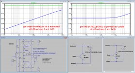
By placing a resistor in parallel, I can investigate the effect of Ro, in this very case using 165K@1mA@1V for the BC550C/BC560C.
When the simulated Ro is infinite (not shown here), gm remains constant at 38mA/V independent of Rload.
But with an accurate calculated value for Ro in the the left part of the image below, results are becoming comparable but not for the full 100%.
Maybe I should make a model with variable Ro for accurately replacing a BC550C/BC560C with all other parameters comparable.
Hans
Attachments

Dishonest CFA's are indexed nowhere.I've made lots of use of this with the AD844. Like with any honest CFA, current at -in = output current at Tz. So you can set voltage gain by the ratio of series R at -in to load R at Tz. Jan
The property of current at -in = output current at Tz you mention is that of a pseudo-ideal transistor (*) using current mirrors and the circuit you describe is without global feedback. It's an evolution of the basic emitter degenerated single transistor.
(*) https://www.edn.com/electronics-blo...ansistor-?utm_source=Aspencore&utm_medium=EDN
Chris,
The anomaly I found in the GP model was specifically the ratio of Ic6/Vbe. When the Tz termination resistance was varied in your test circuit (Post 1872 AD844) Current Feedback Amplifiers, not only a semantic problem? you found a massive unexpected drop from 38mS to 0.15mS!! when this should not change much at all.because you are only altering the termination resistance of the output of the current mirrors and there should be negligible change in the DC bias.
Ian, I see no reason for any change in DC bias, since my load resistor was AC-coupled. Can we agree that the connection of an AC-coupled load in a small signal application should have no effect on the DC bias, and that therefore the DC bias didn't change? Yet you seem to believe that gm (which I believe should always equal I(DC)/ (kT/q)) changed, but agree that this is a mystery even if the VBIS model is used. I don't believe that there was any change in gm or any mystery and that my original explanation is correct. Note that ic/vbe = gm if and only if vce is held constant, which is not the case here. ic/vbe changed; gm did not. Please feel free to poke holes in the following:
What was happening is a consequence of the fact that Ic = gm vbe + vce/ro. These two components of AC current are subtractive at the collector and emitter nodes. This can be seen if we consider the npn inverting input transistor alone. When vb is at the positive peak of an applied input sine wave, vbe is at its maximum, and gm vbe delivers its peak current. At the same time, ve is also at its maximum and so vce is at its minimum (since vc is approximately at AC ground), and so vce/ro delivers its trough current. As the loop gain increases and vbe continues to fall, the two AC current contributions approach approximately equal magnitudes, with the gm vbe component always slightly larger so as to supply the ic needed for the circuit to work.
I don't see how just measuring the Early effect resistance 'ro' relates to this anomaly. I think you would need to make the circuit you simulated and bench test it to find the ratio of Ic/Vbe for Q6 with AC signals.
I hope I have explained why I think the bench test I did was sufficient to explain this effect in conjunction with the simulation and my explanation above.
As I demonstrated with the VBIC model in your circuit the ratio of Ic to Vbe was quite close to the expected constant gm value of 30-40mA/V at 1mA. and that over the wide range of Tz loading resistances.
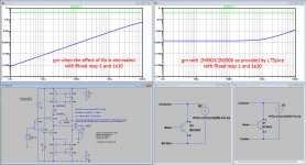
I have since found the VBIC's small spread is mainly determined by the choice of parameter 'mc' which is MJC in the GP (base-collector capacitance exponent). The attached plot shows the two plots with mc=0.75 (earlier BC550C_V was 0.25). I don't understand the theoretical basis why this capacitance parameter affects the Ic/Vbe in this way - charge based models are still a mystery to me. Perhaps someone can explain why it is so from the physics?
You found a change of a factor of 3 rather than one of 300. The mystery is that there is any change at all! If a model's capacitance changes transistor transconductance at 1kHz by a factor of 3, there is a problem with the model, don't you agree? Again, I think that the simpler explanation is that gm as defined above is unchanged and that it is ic6/vbe6 only that changes.
I'm not saying we have to ditch the present GP model in LTspice etc. It's just we cannot use it to resolve the query that CPaul raised concerning the Early effect and the transconductance in the input stage of a CFA. With the VBIC model the gm transconductance of the input stage is seen to be controlling the current to the mirrors. The GP model fails to resolve your query. For most other simulations the GP model is very good.
I disagree with your conclusion for the reasons I mentioned above. I believe that my explanation explains the observed phenomenon, but I am certainly willing to be shown I am wrong and that there is a problem with the models as you claim. The very last thing I want is for this disagreement to escalate into a flame war. The thing I most want is for us to both agree on the correct explanation, and to be cured of any misapprehension I might have.
For me, the first step in this process would be for you to find an error in my explanation. Would you be willing to do this?
A few postings before I measured with LTSpice an Ro value for the BC550 of 165K@1mA and somewhat later 196K@1mA for the 2N3904.
The BC550 value was correct but for the 2N3904 I made a mistake and now measured resp 102K@1mA and 50.3K@2mA.
The early voltage Va (=Ic*Ro-Vc) for a small signal transistor usually seems to be somewhere between 15 and 150 Volt.
With a Va of ca 100 Volt this is the case for the 2N3904 in LTSpice.
But your bench results are quite a bit outside this range with Va > 250 Volt, so are you quite sure about this measurement ?
Hans
It is always possible that there was a measurement error. Perhaps I'll repeat the test depending on how the discussions turn out.
The thing I found interesting is that some references state that hoe = 1/ro should be measured at constant ib (which I did) and others with constant vbe. (I wonder if it makes a difference.) Can anyone speak authoritatively about this? I think I recall Scott having something to say on the matter.
I have made another Sim where the effect Ro in the BC550C/BC560C model has been eliminated by placing a current source par. to Ro, generating an exact opposite current.
By meticulously tuning in finding the Early voltages A and B for both transistors, I get the image below.
I think now the effect of Ro has been eliminated, it becomes quite obvious that Ro is not the cause of measuring different values for gm at differen values for Rload.
Hans
By meticulously tuning in finding the Early voltages A and B for both transistors, I get the image below.
I think now the effect of Ro has been eliminated, it becomes quite obvious that Ro is not the cause of measuring different values for gm at differen values for Rload.
Hans
Attachments
And if this is correct, where did you get the 2N3904? Manufacturer? Transistors with high Early voltage (and thus a high voltage gain limit) are rare these days, it would be nice to know.
Not sure. The marking is 2N3904 followed by a -H18. Got it through Digi-key. Checked some of the mfg. data sheets but I can't find a match.
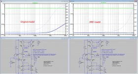
Here is the schematic in single ended inverted form. No Gm anomaly.
No gm anomaly; there never was. However, ic6/vb6 still changes a great deal with Rload.
I don't know why you decided to configure it as an inverter, but ic6/vb6 varies significantly with Rload as both an inverter and as a non-inverter.
As the original non-inverter, with Rload in series with a 1 farad cap, ic6/vbe6 changes from .267uS to 2.99mS when Rload goes from 1mOhm to 1E10 Ohms.
With the new model and Rload = 1 mOhm (no significant AC feedback) ic6/vbe6 = 3mS! Something is not right.
I have made another Sim where the effect Ro in the BC550C/BC560C model has been eliminated by placing a current source par. to Ro, generating an exact opposite current.
By meticulously tuning in finding the Early voltages A and B for both transistors, I get the image below.
I think now the effect of Ro has been eliminated, it becomes quite obvious that Ro is not the cause of measuring different values for gm at differen values for Rload.
Hans
Without reviewing your results, please consider that there is nothing else in the Hybrid Pi model other than ro that could explain this phenomenon.
In the image belonging to the above posting, I have written 2N3904/2N3906.I have made another Sim where the effect Ro in the BC550C/BC560C model has been eliminated by placing a current source par. to Ro, generating an exact opposite current.
By meticulously tuning in finding the Early voltages A and B for both transistors, I get the image below.
I think now the effect of Ro has been eliminated, it becomes quite obvious that Ro is not the cause of measuring different values for gm at differen values for Rload.
Hans
This should of course be BC550C/BC560C.
See corrected image below.
Hans
Attachments
Last edited:
Sorry Chris,Without reviewing your results, please consider that there is nothing else in the Hybrid Pi model other than ro that could explain this phenomenon.
You would be right when the Hybrid Pi model was perfect, but be aware that this Hybrid Pi model is only a simplified model not containing all parameters.
After the contribution of Ro has been eliminated in my Sim, the effect on gm when using a large value for Rload has become even larger instead of smaller, exactly the opposite what should have happened when Ro had been the cause.
So at least within LTSpice there is a more complete Transistor model causing this effect.
And that's why I lost my believe in holding Ro responsible for causing this gm diminishing effect.
Also be aware that in your Sims where you noticed this effect for the first time, the "extra" contribution that LTSpice produces was also part of your result, making it impossible to validate your results.
Maybe it's not a bad idea after all to see what a VBIC model could make of all this.
Hans
Last edited:
Sorry Chris,
You would be right when the Hybrid Pi model was perfect, but be aware that this Hybrid Pi model is only a simplified model not containing all parameters.
After the contribution of Ro has been eliminated in my Sim, the effect on gm when using a large value for Rload has become even larger instead of smaller, exactly the opposite what should have happened when Ro had been the cause.
So at least within LTSpice there is a more complete Transistor model causing this effect.
And that's why I lost my believe in holding Ro responsible for causing this gm diminishing effect.
Hans
Hans, please discriminate between ic/vbe and gm. Even if the Early effect does not explain the phenomenon we are discussing, it does exist, and so gm = I(DC) / (kT / q)and ic/vbe are not the same thing.
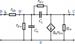
Yes, Hybrid Pi does not explain everything, so there might be something else going on. But it is derived from the Ebers-Moll and Early equations/models. Attached is a more complete H-pi model. the text that goes along with its is:
Full hybrid-pi model
The full model introduces the virtual terminal, B', so that the base spreading resistance, rbb, (the bulk resistance between the base contact and the active region of the base under the emitter) and rb'e (representing the base current required to make up for recombination of minority carriers in the base region) can be represented separately. Ce is the diffusion capacitance representing minority carrier storage in the base. The feedback components, rb'c and Cc, are introduced to represent the Early effect.
So perhaps you are not compensating for the full effect. I know I haven't considered rb'c and Cc, although I expect that Cc's effect at 1kHz would be small.
Attachments
- Home
- Amplifiers
- Solid State
- Current Feedback Amplifiers, not only a semantic problem?