Hi Berny,
glad you enjoy the music daily ! 🙂
There's been more stuff since Cubie3, it will be published eventually...
All the best !
Thank you Juma 🙂
Maybe I should wait to see juma's newest amp before making up more pcb's. The main reason I drew up a manufactured pcb was to enable anyone who cannot etch his own pcb to enjoy this build.
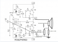
juma: Does some of your new stuff include putting Positive Current Feedback onto a cubie3? I was thinking the attached sketch that Circlomanen made in the F6 with PCF thread might work great on a cubie3. I would think a R-Sense of 1 ohm might be a good starting point since there is more gain in a cubie3. Your thoughts?
Attachments
No need for that in Cubie3. Zout is already very low (i.e. dumping factor is high).
The PCF is not an universal cure - more like a poison that can bring some improvement in very specific cases.
F6 looks like a good candidate for PCF implementation, but I got better results with gain stage instead of a buffer and nesting the F6 inside its feedback loop.
Of course, feel free to make your own experiments...
Calculation of R4 and R6
Hello
I put this circuit together during the weekend but I am not able to calculate the values for R4/R6. My jfets are a matched pair with 8.2ma Idss.
Can someone help me?
I am also running the circuit +-25 power supply and changed r16/r18 to 10k.
Hello
I put this circuit together during the weekend but I am not able to calculate the values for R4/R6. My jfets are a matched pair with 8.2ma Idss.
Can someone help me?
I am also running the circuit +-25 power supply and changed r16/r18 to 10k.
Well it did not
I tested the circuit today.
Feedback resistors got very hot and I had positive rail voltage on output.
Both channels exhibit the same symptoms.
I hope I did not burn the input fets our the output fets.
I doublechecked the connections and measured the resistors and no problem there.
I am just wondering what could cause this.
My schema and board as attachment.
Attachments
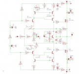
Sorry jarkaa but I can't check your layout, it's too small and messy for me - grid, writings, mixed colors (I'm plain vanilla type - black traces on white paper with red parts ...)
Check your parts' values, polarity and orientation (transistors especially, it's so easy to turn them the other way around). 68R in current mirrors will make the gm stage current too low.
Did you connect signal ground to power ground ? Without that connection, the circuit will behave exactly as you described it.
Hello Juma,
Thanks for your comments.
The signal ground is routed directly between the main caps in the power supply so there should be no problem with that.
Transistors has been checked and should be oriented according to the schema / layout. Allthough the source of the transistors is unknown. I found a bag from my part drawer and used those.
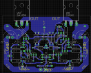
I Attached a new layout, I hope it is more readable. I am not completely familiar with new eagle...
Also I am out of the small transistors right now so I need to order some more.
Br,
J
Thanks for your comments.
The signal ground is routed directly between the main caps in the power supply so there should be no problem with that.
Transistors has been checked and should be oriented according to the schema / layout. Allthough the source of the transistors is unknown. I found a bag from my part drawer and used those.
I Attached a new layout, I hope it is more readable. I am not completely familiar with new eagle...
Also I am out of the small transistors right now so I need to order some more.
Br,
J
Attachments
Last edited:
Layout looks ok.
Maybe some of the small bjts are out of spec or bad - I check every part before I solder it .
If you are going to buy new bjts take ON semiconductor or Fairchild from reliable source (mouser, digikey...).
A lot of good projects ended in trash bin because of cheap/fake parts from ebay/china...
Maybe some of the small bjts are out of spec or bad - I check every part before I solder it .
If you are going to buy new bjts take ON semiconductor or Fairchild from reliable source (mouser, digikey...).
A lot of good projects ended in trash bin because of cheap/fake parts from ebay/china...
Hi Juma,
I'm considering to etch a pair of boards to test the Cubie3 in comparison with some others which will use the same power supply at +/-36V.
Your original schematic at post #1 you make use of GR grade of Jfets but I only have BL grade with Idss=8-8.5mA and the GR are difficult to find in the market.
As far as I can understand, in order to make use of such Jfets, I would increase the values of the resistors R6 and R4 (68-82R) to get about 5ma flowing through Q5/Q8.
Am I right? Do you think I should change something more or different?
Many thanks in advance for your help and suggestions
Nicola
Yes you are. We don't want to overheat Q5/Q8. I told jarkaa not to change those resistors because he intended to use +/-25V power supply....Am I right?
More capacitance in power supply is a usual target. Actually, feel free to change anything you consider necessary. 🙂Do you think I should change something more or different?
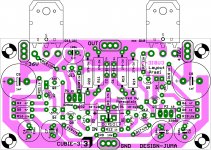
@prasi,
Can you share original eagle cad files of your layout?
I need to modify board dimension to fit TO3 output devices on existing heatsink.
Can you share original eagle cad files of your layout?
I need to modify board dimension to fit TO3 output devices on existing heatsink.
@prasi,
Can you share original eagle cad files of your layout?
I need to modify board dimension to fit TO3 output devices on existing heatsink.
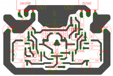
here you go...All the best for your build. I had a wrong pin device for K170 in the earlier posted layout (pointed out by Juma).
I have it corrected in the attached sch and brd.
All the best for your build.
reg
Prasi
Attachments
Maybe....
I don't know what your goal is, what speakers you have, your budget, listening preferences, what parts you want to use/already have, etc ....
I don't know what your goal is, what speakers you have, your budget, listening preferences, what parts you want to use/already have, etc ....
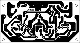
Hi
Can someone confirm these layouts are correct or not. I plan to etch some PC boards, my friend would love to build these amp. So he ask me etch a pair PC boards.
If someone built and test it one of these boards please let me know
I would love to use the correct layout otherwise it will be a waste.
By the way Prasi what is the actual size of the boards, I found out one is your design.
Thank you very much
Greetings to all 🙂
Attachments
- Home
- Amplifiers
- Pass Labs
- Cubie3