Elementary, my dear Watson. 🙂
The sources are low Z feedback nodes (the spot where R1 meets R14/R13 and where R2 meets R11/R22).
If the part is marked as 2sk170 (N-channel JFET, says the datasheet) and we see that gate receives the input signal and one of the pins connects to ground through a small value resistor while the other mystery pin strives towards higher potential it's pretty easy to identify them all (assuming one knows basic stuff about JFETs).
So, knowing how parts work is always beneficial although I completely understand that soldering is much more fun than reading and thinking, but one has to accept that there is a price to be paid when such an approach is used... 😉
BTW, not all JFETs are symmetrical. Some are symmetrical only under certain conditions.
Even more elementary, dear Sherlock, you labelled the layout in the first post. Did't think to look lil I went back and looked at the Cubie2 thread to compare. Escaped thinking once again. 
Never you mind - you know what they say: a month in a workshop can save you a day in a library! 😀
Keep up the good work,as long as the smoke stays contained inside the parts you are doing great !
Keep up the good work,as long as the smoke stays contained inside the parts you are doing great !
marsupialx: A little trick I use to remember, which you might like is: on a FET if the arrow point iN then it is an N channel and the Negative electrons flow from the side (or leg) that is more Negative, which is its Source, to the side that is more positive, which is its Drain. Notice all the places that the letter N is capitalized. Note that both sides may be negative or positive in relation to ground.
If the arrow points out, then it is a P channel and the Positive holes flow from the side that is more Positive, which is its Source, to the side which is more negative, which is its Drain. It is understood that a hole flowing one direction means an electron is flowing the other direction.
Thank you for drawing that layout, I am sure a lot of people will appreciate it.
marsupialx: A little trick I use to remember, which you might like is: on a FET if the arrow point iN then it is an N channel and the Negative electrons flow from the side (or leg) that is more Negative, which is its Source, to the side that is more positive, which is its Drain. Notice all the places that the letter N is capitalized. Note that both sides may be negative or positive in relation to ground.
If the arrow points out, then it is a P channel and the Positive holes flow from the side that is more Positive, which is its Source, to the side which is more negative, which is its Drain. It is understood that a hole flowing one direction means an electron is flowing the other direction.
Thank you for drawing that layout, I am sure a lot of people will appreciate it.
Thanks for the mnemonic! My brain needs devices such as this to slowly "get it". It ever so slowly gets less frustrating. I'm a long way from designing, but I am more and more able to isolate the piece of the puzzle that I am in need of. Thanks again!!!
In this case, I wanted to make sure, because it's not just my parts that would give up the magic blue smoke. Ok, fellow thought avoiders, here's the part stuffing guide.
Thanks!!
In this case, I wanted to make sure, because it's not just my parts that would give up the magic blue smoke. Ok, fellow thought avoiders, here's the part stuffing guide.
Hi,
I was making a layout for this amp, and noticed that P2 and R8 connection is not as per schematic. May be it doesnt matter as they are in series. could you confirm?
reg
Prasi
That made me scratch my head as well. They are in series, don't much matter which sits where. juma does that kind of stuff. It's like he wants us to think or something. Just finished stuffing my boards. Have yet to plug the sucker in. Tomorrow.
No, really. It just looked more convenient when I drew the board since it doesn't matter. P2+R8 make a composite resistor consisting of one fixed value resistor and one trimm pot connected in series so you can turn them any way you want and the resulting resistance will still be the same...That made me scratch my head as well. They are in series, don't much matter which sits where. juma does that kind of stuff. It's like he wants us to think or something. Just finished stuffing my boards. Have yet to plug the sucker in. Tomorrow.
cubie-3 layout
Hi Juma and Marsupialx,
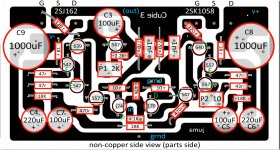
Here is the first draft of layout of cubie-3 by me. It is inspired by marsupialx's layout, but I tried to use all horizontally mounted resistors and without piggy-backing and bigger caps (hopefully, as i didnt have the original layout). This was required by a forum member.
Size of course is compromised [bigger😱PCB ]and also also no match for curved traces on marsupialx's layout🙂.
I will keep trying to reduce size further, but would like to have comments on the layout for any gross mistakes regarding unacceptable trace lengths/widths, etc especially around i/p section. Schematic and layout consistent. 24mils spacing min and 0.635mm annular ring on pads.
reg
Prasi
Hi Juma and Marsupialx,
Here is the first draft of layout of cubie-3 by me. It is inspired by marsupialx's layout, but I tried to use all horizontally mounted resistors and without piggy-backing and bigger caps (hopefully, as i didnt have the original layout). This was required by a forum member.
Size of course is compromised [bigger😱PCB ]and also also no match for curved traces on marsupialx's layout🙂.
I will keep trying to reduce size further, but would like to have comments on the layout for any gross mistakes regarding unacceptable trace lengths/widths, etc especially around i/p section. Schematic and layout consistent. 24mils spacing min and 0.635mm annular ring on pads.
reg
Prasi
Attachments

Applied power, measuring the amperage on the positive power lead. I get 1 amp (1.092 and 1.047). Turning the pots doesn't seem to affect it. What reading would be desirable, or any thoughts on what to change? Built with BC550 and BC560. Everything else is stock. Thanks!!!
Very nice. Far more "conventional" than I seem to pull off. Looks very straight forward, unlike my prettied up sharpie marker layout aesthetic. Resistors can actually lie flat. What a concept. I like it. I'm tempted to build another, but I better get this one working, first.😀 I see little need to reduce the size.Hi Juma and Marsupialx,
Here is the first draft of layout of cubie-3 by me. It is inspired by marsupialx's layout, but I tried to use all horizontally mounted resistors and without piggy-backing and bigger caps (hopefully, as i didnt have the original layout). This was required by a forum member.
Size of course is compromised [bigger😱PCB ]and also also no match for curved traces on marsupialx's layout🙂.
I will keep trying to reduce size further, but would like to have comments on the layout for any gross mistakes regarding unacceptable trace lengths/widths, etc especially around i/p section. Schematic and layout consistent. 24mils spacing min and 0.635mm annular ring on pads.
reg
Prasi
Hi Juma and Marsupialx,
Here is the first draft of layout of cubie-3 by me. It is inspired by marsupialx's layout, but I tried to use all horizontally mounted resistors and without piggy-backing and bigger caps (hopefully, as i didnt have the original layout). This was required by a forum member.
Size of course is compromised [bigger😱PCB ]and also also no match for curved traces on marsupialx's layout🙂.
I will keep trying to reduce size further, but would like to have comments on the layout for any gross mistakes regarding unacceptable trace lengths/widths, etc especially around i/p section. Schematic and layout consistent. 24mils spacing min and 0.635mm annular ring on pads.
reg
Prasi
Hi
Did someone tested these layout
If yes are you willing to share it with us, it does look nice! 🙂
Greetings
Thanks, you better get yours working first, coz mine is based on your layout.
just kidding,thanks anyway. you are most welcome to try after you get yours working😉.
reg
prasi
are you indulging in self-praise😀? I thought I did that by giving due credit and also the praise regarding the the trace curves😀.Far more "conventional" than I seem to pull off. Looks very straight forward, unlike my prettied up sharpie marker layout aesthetic. Resistors can actually lie flat. What a concept.
just kidding,thanks anyway. you are most welcome to try after you get yours working😉.
reg
prasi
hi,Hi
Did someone tested these layout
If yes are you willing to share it with us, it does look nice! 🙂
Greetings
no, not tested, but as said in above posts, I based mine marsupialx's layout. of course i will share, once i get people's comments. only if someone could go over it with a
 from design point of view.
reg
Prasi
Last edited:
Thanks, you better get yours working first, coz mine is based on your layout.
are you indulging in self-praise😀? I thought I did that by giving due credit and also the praise regarding the the trace curves😀.
just kidding,thanks anyway. you are most welcome to try after you get yours working😉.
reg
prasi
No indulging on my part. I don't seem to be able to break out of the Cubie tradition of having a super compact board. With your layout, I like a little breathing space in there. As for getting it to work, I take some consolation in the two channels being in the same ball park. I don't know for sure if my latfets are genuine. Time to figure out what's going on. You don't need to credit me on the layout. It's juma's baby.
Last edited:
Turning the P1 should change the Vgs of Q10/Q11.Applied power, measuring the amperage on the positive power lead. I get 1 amp (1.092 and 1.047). Turning the pots doesn't seem to affect it. ...
Set DC voltmeter to 20V range.
Put one probe on the gate of Q10 and the other on the gate of Q11. The meter will show some voltage and that voltage should change as you turn P1. If not, you messed something up.
Check if transistors are in proper places and properly oriented.
- Home
- Amplifiers
- Pass Labs
- Cubie3