I have a power transformer. 44V CT secondary, 160VA. Is it suitable for cubie3? Could you kindly advise what adjustment to make on the circuit?
Thanks.
Regards,
Tat
Thanks.
Regards,
Tat
44V AC CT is OK. Make R16, R18 = 15k
Read carefully post #1, especially 4th paragraph (measure your JFETs' Id at 10V Vds with 10R degeneration - the value of R4, R6 will depend on that).
Edit: Actually, if you plan to use the PSU from post #1 (cap multiplier), make R16, R18 = 12k
Read carefully post #1, especially 4th paragraph (measure your JFETs' Id at 10V Vds with 10R degeneration - the value of R4, R6 will depend on that).
Edit: Actually, if you plan to use the PSU from post #1 (cap multiplier), make R16, R18 = 12k
Last edited:
I am having trouble locating BC639. There is a BC63916 that looks similar. Is it similar enough, or should I continue my quest for BC639. Thanks!!!
Take BD13916 and BD14016 - it's the same thing in TO-126 package and both are made by Fairchild (suffix 16 means higher hfe).
That way the current through them can be raised to 10 ma and two pairs of output Lateral MOSFETs can be easily driven (if you wish that. But in that case your PSU should be up to it - you'll need 400VA transformer and double the filter capacitance).
That way the current through them can be raised to 10 ma and two pairs of output Lateral MOSFETs can be easily driven (if you wish that. But in that case your PSU should be up to it - you'll need 400VA transformer and double the filter capacitance).
Hi Juma,
If you don't mind, could you share the main reasoning for the change of the current mirror topology from cubie2 to cubie3, is it supply related or sonic issue? Which one would you recommend to use for a build utilizing F5 style 20-22V dual supply?
If you don't mind, could you share the main reasoning for the change of the current mirror topology from cubie2 to cubie3, is it supply related or sonic issue? Which one would you recommend to use for a build utilizing F5 style 20-22V dual supply?
Perhaps a little misunderstanding, my first question was not about how to calculate biases, it was about your personal reason behind the choice of topology change, between regular current mirror with hawksford cascode and wilson mirror. But anyway, more important to me is the answer you gave for the second question. Thank you.
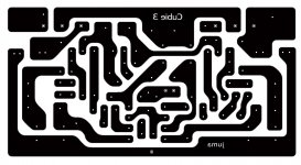
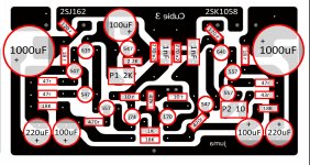
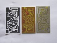
Just finished making the Cubie 3 PCB's.
🙂
Looks good! But I might be biased.
No. First post, second paragraph says it roughly - you are lazy to read as much as I'm lazy to type... 🙂Perhaps a little misunderstanding, ...
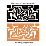
Did you do the boards photoresist etch or iron transfer?Just finished making the Cubie 3 PCB's.
🙂
The reason I ask is the laser printout seems correct for transfer etching, but your board looks the same as the laser print, and it should be a mirror image. Just to avoid weirdness, look at it and make sure it is correct. If it is mirrored, you will have to pay very close attention to all polarities during build.
Last edited:
Thanks Juma, that explains it for me. I don't think I get it yet, but I think I'll understand better in time after working a bit more on it.First post, second paragraph says it roughly . . .

Hi Marsupialx,
I used the photoresist etch method to make the PCB's. I may have to make new PCB's, messed up a couple of traces during drilling, my eyes are not as good as they use to be. 😉 I will email you the details.
Thanks.
I used the photoresist etch method to make the PCB's. I may have to make new PCB's, messed up a couple of traces during drilling, my eyes are not as good as they use to be. 😉 I will email you the details.
Thanks.
Another option is to build it inserting the parts on the copper trace side. The only problem is electro caps, since they block the solder pads if inserted fully. If one left just enough space to carefully solder them, and then use silicone to fill in the space, or let them stand on their leads (which could vibrate), one could populate a backwards board. I re-etched the Slewmaster board I originally etched backwards. Ps, the type (cubie3 and juma) should read correctly on the copper side.
Ok, time for yet another question. Jfets are symmetrical. Is their no preferred orientation? The schematic diagram doesn't seem to indicated which is drain and which is source. I know which is which looking at the actual device, but I don't get how to tell looking at a schematic. Thanks!!
- Home
- Amplifiers
- Pass Labs
- Cubie3