I am happy with LTspice'ing..
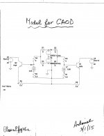
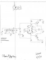
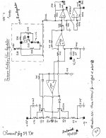
Because the model and the prototype are on the same page, and of its unexpected revelations. The left image is the schematic of of CAOD. Please note the following additions to the schematic of the previous post.
1.The voltage generator V4 at the bottom-middle of the schematic. It is equivalent to the input voltage to the non-inverting port of the amp. Note that both BJTs are fed from it simultaneously; meaning in-phase.
2. The dummy load R7 = 4 Ohms.
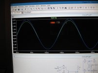
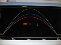
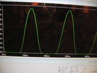
I had previously thought that Vout across the load is 8 Vp-p and still keeps the BJTs from crossing-over. I was wrong. This model and the proto show that it can only be 1 Vp-p as seen on the photo [of laptop screen] of the following performance.
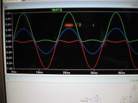
1. The green trace is the voltage at the emitter of NPN. It is equivalent to a positive-going 1/2 wave rectified string of pulses [1 Vp]. NPN turns off; but does not cross-over below the 0 V plateau..
2. The middle blue trace is the Vout sine wave at R7 [1Vp-p].
3. The pink negative going trace is the voltage at the emitter of PNP [-1Vp]. PNP turns off; but does not crossover above the 0V plateau.
4. One can readily push both BJTs to crossover [slight excursion into Class B] by increasing the amplitude of V4 say from 0.5 to 0.7 Vp.
Analysis: This amp wastes a lot of current ; meaning it has a poor efficiency as follows; say in the time duration of 0 to 10 milliseconds.
1. A 0.5 Vp across 4 Ohms is 0.125A.
2. A 0.5 Vp across the 0.5 Ohm emitter resistor of NPN [numerical difference between shown green and blue peaks] gives 1 Ap.
3. The efficiency is a poor 12%.
4. The difference or balance of the current [1 Ap-0.125 Ap] is dissipated in PNP. Click on its collector node to find it across the sense resistor of 0.5 Ohms.
Here is how it works. As the sine wave at V4 goes positive [+0.5 Vp] it adds to the positive going FWAPs [0.5 Vp] at the base of NPN to give 1 Vp net. It also simultaneously adds to the negative going FWAPs [-0.5Vp] at the base of PNP [to give a 0 Vp net.
Best regards.
Because the model and the prototype are on the same page, and of its unexpected revelations. The left image is the schematic of of CAOD. Please note the following additions to the schematic of the previous post.
1.The voltage generator V4 at the bottom-middle of the schematic. It is equivalent to the input voltage to the non-inverting port of the amp. Note that both BJTs are fed from it simultaneously; meaning in-phase.
2. The dummy load R7 = 4 Ohms.
I had previously thought that Vout across the load is 8 Vp-p and still keeps the BJTs from crossing-over. I was wrong. This model and the proto show that it can only be 1 Vp-p as seen on the photo [of laptop screen] of the following performance.
1. The green trace is the voltage at the emitter of NPN. It is equivalent to a positive-going 1/2 wave rectified string of pulses [1 Vp]. NPN turns off; but does not cross-over below the 0 V plateau..
2. The middle blue trace is the Vout sine wave at R7 [1Vp-p].
3. The pink negative going trace is the voltage at the emitter of PNP [-1Vp]. PNP turns off; but does not crossover above the 0V plateau.
4. One can readily push both BJTs to crossover [slight excursion into Class B] by increasing the amplitude of V4 say from 0.5 to 0.7 Vp.
Analysis: This amp wastes a lot of current ; meaning it has a poor efficiency as follows; say in the time duration of 0 to 10 milliseconds.
1. A 0.5 Vp across 4 Ohms is 0.125A.
2. A 0.5 Vp across the 0.5 Ohm emitter resistor of NPN [numerical difference between shown green and blue peaks] gives 1 Ap.
3. The efficiency is a poor 12%.
4. The difference or balance of the current [1 Ap-0.125 Ap] is dissipated in PNP. Click on its collector node to find it across the sense resistor of 0.5 Ohms.
Here is how it works. As the sine wave at V4 goes positive [+0.5 Vp] it adds to the positive going FWAPs [0.5 Vp] at the base of NPN to give 1 Vp net. It also simultaneously adds to the negative going FWAPs [-0.5Vp] at the base of PNP [to give a 0 Vp net.
Best regards.
Attachments

LTspice model gives additional ..
Insight, knowledge and direction. I need two posts to elaborate a graphic comparison of the performance of Class A on Demand [CAOD] versus Class AB. This post talks about:
1. CAOD
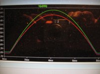
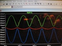
2. I've increased the power output voltage to 8 V peak to peak from the inefficient 1 V peak to peak of the previous post.
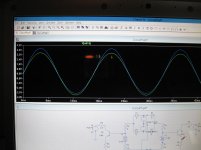
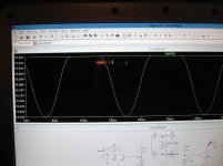
The left image shows a green AC signal at Vo, and a blue AC signal at the emitter of NPN. The analysis equally applies to PNP.
1. Focus at both of the positive- going peaks at ~4 millisecs. The difference between the peak voltages at this time is the voltage drop across the 0.5 Ohms NPN emitter resistor; which is then used to calculate the peak current flowing through it.
2. Focus next at both of the negative-going peaks at ~12 millisecs. There is a difference in the peak voltages. It follows that there is a voltage drop across the 0.5 Ohm emitter resistor of NPN which further says that current is flowing through it and that NPN is turned on. The underlined is a significant find which is further emphasized by the trace of the right image as follows.
3. The trace is at the collector of NPN; effectively across its 0.5 Ohm resistor which senses collector current. Note the peak at ~ 12 millisecs which is the voltage drop across its 0.5 Ohm sense resistor, and thus means that NPN is turned ON when it should be turned off in the comparison model of Class AB.
4. The implication is that I am now able to increase the efficiency of CAOD; from the mediocre 1 Vp-p of the previous post to 8 Vp-p; because NPN [and ditto for PNP] do not turn off which is the objective of this application.
I'll show in the next post graphs taken at the same ports of NPN comparing and analyzing Class AB.
Insight, knowledge and direction. I need two posts to elaborate a graphic comparison of the performance of Class A on Demand [CAOD] versus Class AB. This post talks about:
1. CAOD
2. I've increased the power output voltage to 8 V peak to peak from the inefficient 1 V peak to peak of the previous post.
The left image shows a green AC signal at Vo, and a blue AC signal at the emitter of NPN. The analysis equally applies to PNP.
1. Focus at both of the positive- going peaks at ~4 millisecs. The difference between the peak voltages at this time is the voltage drop across the 0.5 Ohms NPN emitter resistor; which is then used to calculate the peak current flowing through it.
2. Focus next at both of the negative-going peaks at ~12 millisecs. There is a difference in the peak voltages. It follows that there is a voltage drop across the 0.5 Ohm emitter resistor of NPN which further says that current is flowing through it and that NPN is turned on. The underlined is a significant find which is further emphasized by the trace of the right image as follows.
3. The trace is at the collector of NPN; effectively across its 0.5 Ohm resistor which senses collector current. Note the peak at ~ 12 millisecs which is the voltage drop across its 0.5 Ohm sense resistor, and thus means that NPN is turned ON when it should be turned off in the comparison model of Class AB.
4. The implication is that I am now able to increase the efficiency of CAOD; from the mediocre 1 Vp-p of the previous post to 8 Vp-p; because NPN [and ditto for PNP] do not turn off which is the objective of this application.
I'll show in the next post graphs taken at the same ports of NPN comparing and analyzing Class AB.
Attachments
More insights from LTspice model
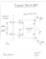
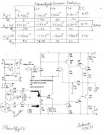
The performance of the comparison Class AB follows. But first, cut the lines [wires] in the model of CAOD of the previous post which feed the Full Wave Analog Pulses [FWAP] to the bases of the BJTs. One is thus left with a Class AB amp for evaluation.
The left image shows the following:
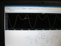
1. The green AC signal is Vo across 4 Ohms dummy load.
2. The blue AC signal is the signal at the emitter of NPN.
3. Focus at the positive-going peaks at ~4 millisecs. The difference in their voltages is the voltage drop across the 0.5 Ohm emitter resistor of NPN.
4. Focus next at the negative-going peak at ~12 millisecs. There is only one single peak; meaning there is no longer a voltage drop across the same 0.5 Ohm emitter resistor like for the positive-going peaks. No current flows through this resistor; meaning NPN is turned off as it should in Class AB.
5. Note the both AC signals began merging into one negative-going signal at slightly below 0V as it should in Class AB.
6. The right image shows performance at the collector of NPN as sensed by its 0.5 Ohm resistor. NPN is fully on at 4 millisecs as it should and is fully off in the plateau centered at 12 millisecs.
7. The above analyses are identical for PNP.
I'll increase V4 [input signal] in the model of CAOD to levels greater 8 V-p-p [used in this and the previous post] to note [graphically] the turning off the conduction point of NPN.
Next up is for me to learn from Mooly's thread [on learning LTspice] and others on the web how to determine objective performance like THD etc. for CAOD and its comparison Class AB amp.
sO
The performance of the comparison Class AB follows. But first, cut the lines [wires] in the model of CAOD of the previous post which feed the Full Wave Analog Pulses [FWAP] to the bases of the BJTs. One is thus left with a Class AB amp for evaluation.
The left image shows the following:
1. The green AC signal is Vo across 4 Ohms dummy load.
2. The blue AC signal is the signal at the emitter of NPN.
3. Focus at the positive-going peaks at ~4 millisecs. The difference in their voltages is the voltage drop across the 0.5 Ohm emitter resistor of NPN.
4. Focus next at the negative-going peak at ~12 millisecs. There is only one single peak; meaning there is no longer a voltage drop across the same 0.5 Ohm emitter resistor like for the positive-going peaks. No current flows through this resistor; meaning NPN is turned off as it should in Class AB.
5. Note the both AC signals began merging into one negative-going signal at slightly below 0V as it should in Class AB.
6. The right image shows performance at the collector of NPN as sensed by its 0.5 Ohm resistor. NPN is fully on at 4 millisecs as it should and is fully off in the plateau centered at 12 millisecs.
7. The above analyses are identical for PNP.
I'll increase V4 [input signal] in the model of CAOD to levels greater 8 V-p-p [used in this and the previous post] to note [graphically] the turning off the conduction point of NPN.
Next up is for me to learn from Mooly's thread [on learning LTspice] and others on the web how to determine objective performance like THD etc. for CAOD and its comparison Class AB amp.
sO
Attachments
Thanks to DIYer Mooly..
For his clear and detailed thread [in Software Tools] teaching LTspice. I now have the objective performance [FFT]comparison of Class A On Demand [CAOD] and that of its sub-circuit Class AB. This post shows [only for clarity] the FFT graph and resultant numerical %THD of ~0.13% for CAOD.
The next post will show the comparative performance for the Class AB sub-circuit of CAOD. The Class AB sub-circuit means that the Full Wave Rectifier in CAOD was disabled and all remaining circuit parameters were left untouched.
Best regards.
Attachments

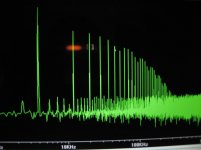
The images below pertain to the performance of Class AB sub-circuit [LTspice model] comparison amp to that of its partner CAOD of previous post. The FFT profile is a bit different from that of CAOD, and its resultant %THD was a bit higher at ~0.3%
The objective results in this and the previous posts suggest that both amps will perform in a satisfactory subjective manner despite these slight differences. Fortunately, it is easy for me to do a subjective listening comparison [sequential] using the actual prototype to probe this proposed result.
I will also do the experiment which Mr. Pass taught in his article Mosfet Citation 12 to see distortion on the scope. One amp in my experiment [Amp A] is Threshold S/150 to drive via an 8 Ohm power resistor the power output node of Amp B which is CAOD or its Class AB sub-circuit as prescribed.
I also have a second experiment prescribed by Mr. David Hafler in an article which he entitled Nulling Out Amp Distortion [Audio/February 1987]. It delves in a similar subject.
Best regards.
Attachments
Just curious and maybe I missed it
What is the load and output voltage swing for the ffts ?
My mistake, I did not show both. Please find attached the LTspice schematic of CAOD which shows that the load is 4 Ohms and the voltage swing across it is ~10 Vp-p from the values of V4 = Vin. I refined this schematic by drawing it the formal way with the signal inputs on its left, and its output stage on the right. I got better at manipulating LTspice.
Please note that the schematic as shown is for the Class AB sub-circuit. It follows that the top simulation command on the bottom left of the schematic [.four..] must have the label for the power output node as n008. After connecting resistors R10, and R11 to the full wave rectifier to simulate CAOD, the new label for the power output node in this command needs to be n007.
The simulation commands are those taught by Mooly at a frequency of 4KHz.
Best regards
Attachments
I concluded in post #115 that this approach of Class A On Demand has a broader reach [imho] into other amp topologies. LTspice is a great tool to tackle this with a theoretical model which I have not built.
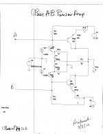
The right image shows the schematic of a model Class AB power amp. It is a BJT abstraction of a diyF5.
1. It has a voltage gain of 5.
2. The darlingtons were a substitute for Mosfets which were troublesome to insert in this schematic.
3. For the interested DIYers, this stand alone model runs trouble-free all the way to include FFTs, and %THDs [forthcoming].
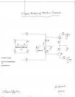
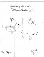
The left image is an LTspice model schematic for the generator of a pair of balanced full wave analog pulses [BFWAP] which are referenced to the power rails [AC common].
1. A run of this model gave FWAPs like I sketched.
2. Note that I left in this schematic of BFWAP the load resistors R2 and R3 [common with right schematic] so as to enable the interested DIYer to view the pulses under simulated conditions.
3. The left of this schematic shows the origin of the FWAPs which is a full wave diode rectifier.
In the upcoming post, I will join these two schematics [at points A and B], and run with the resultant Class A On Demand amplifier all the way to comparative FFTs and % THDs.
Best regards.
The right image shows the schematic of a model Class AB power amp. It is a BJT abstraction of a diyF5.
1. It has a voltage gain of 5.
2. The darlingtons were a substitute for Mosfets which were troublesome to insert in this schematic.
3. For the interested DIYers, this stand alone model runs trouble-free all the way to include FFTs, and %THDs [forthcoming].
The left image is an LTspice model schematic for the generator of a pair of balanced full wave analog pulses [BFWAP] which are referenced to the power rails [AC common].
1. A run of this model gave FWAPs like I sketched.
2. Note that I left in this schematic of BFWAP the load resistors R2 and R3 [common with right schematic] so as to enable the interested DIYer to view the pulses under simulated conditions.
3. The left of this schematic shows the origin of the FWAPs which is a full wave diode rectifier.
In the upcoming post, I will join these two schematics [at points A and B], and run with the resultant Class A On Demand amplifier all the way to comparative FFTs and % THDs.
Best regards.
Attachments
The attached image shows the resultant LTspice model schematic of the so-called Class A On Demand [CAOD] power amplifier. Please note the commands [thanks to DIYer Mooly's lesson on LTspice] in the left bottom of the image. They run the model trouble-free all the way to FFTs and % THD.
Here are 3 basic games to play this model. Game 1 is:
1. Ground Point C which is in the circuit of the full wave rectifier on the left of the image, One gets a Class AB sub-circuit. The commands run it trouble-free FFTs, and a<0.1 % THD.
2. View the signal at the emitter of the NPN Darlington [at R8 = 1 Ohm]. It shows that this BJT is turned off early on [a plateau at 20 V]. One may need to use a simple command like [tran 2 ms] instead of the shown shown set.
Game 2. disconnects points C at the full wave rectifier from common to enable the operation of the generator of the balanced full wave analog pulses. This is the LTspice model of CAOD. Please note the following
1. The quiescent [idle ] conditions of the Class AB sub-circuit are not perturbed
2. The shown set of commands ran this model all the way to FFTs, and a <0.1% THD across the dummy load of 8 Ohms at Vo which was numerically smaller [trivial] than found above.
3. Like above, take a look at the signal found at the emitter of the NPN Darlington [R8] for comparison. The FWAP pulses forced this BJT not to shut off throughout the AC cycle.
4. In this game, the value of resistor R5 [shown as 2 Ohms at Q1 NPN] has a direct impact on the shape of the pulse signal at the emitter of NPN Darlington. I started with a value of R5 equal to 0.6 Ohms and increased it with in-between performance checks on %THD.
Game 3 is to ground the input signal at V8 and enable the operation of BFWAP only. Note the FWAPs at the emitters of the BJT Darlingtons.
I am switched on LTspice ....
Attachments
I reported in error [post #129] a voltage gain for the Class AB amp of 5 instead of the correct 11.
10. I have an experiment to prove the above objective performance which which I'll gladly report in a future post.
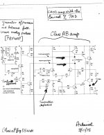
I was not practicing LTspice when I wrote post#115. The above excerpt from its post had emanated from an experiment I did on the prototype to show and prove [to myself] that the power output BJTs do not turn off in operation. The attached images are LTspice models which explain the experiment, further show the met objective and demonstrate the utility of LTspice in my endeavors.
The left image shows the model LTspice schematic under study. On its right is the model schematic of a Class AB amp. The voltage input [to the bases of BJTs] [V4] is rectified by diode D2 to give half wave rectified analog pulses at point C.The left part of the schematic is the generator of balanced half wave analog pulses [BHWAP] at points A [positive-going to NPN], and at point B [negative-going to PNP]. These BHWAPs adjust/increase the current bias of the BJTs in a dynamic sense during the processing of the input signal at point C; so as to meet the objective.
Let's look at the graphic LTspice output in the middle image.
1. All signal generators are enabled at points A, B and C. This is a Class A On Demand amplifier.
2. The green trace is the output signal at the emitter of NPN [most positive amplitude]
3. The blue trace is the power output signal across the dummy load resistor [4 Ohms]. Convention dictates that its amplitude is less than the green trace.
3. The red trace is the amplitude of the signal at the emitter of PNP. The difference in the signal amplitudes of red and blue is a voltage drop across the 0.5 Ohm emitter of PNP. It follows that a current flows through PNP, and thus PNP is active at the signal peaks
4. Roll back to the baseline [right or left] and note that there is still a voltage difference [e.g. at <1 msec] between the red and blue traces. This voltage gap exists throughout the positive going signal. It follows that PNP is on through out the positive-going cycle in CAOD; contra to it shut off in Class AB as follows.
The right-most LTspice scope graphic pertains to Class AB only.
1. Disable BHWAPs at points A and B in the far lest schematic. Left behind is a Class AB model amp which is processing a positive-going half wave rectified pulses at point C [its input].
2. The tallest green trace is the signal at the emitter of NPN.
3. The blue and the red signals have merged into one. This shows/means that PNP is shut off at the peak as it should; because there is no voltage difference across its 0.5 Ohm resistor.
4. Roll back to the traces at <1 msec and note that the blue and the red traces began to merge early on at ~+0.8 Vp; the onset voltage to shut off PNP.
I was happy with this LTspice model [compare CAOD with Class AB] because it is commensurate with the actual test I had done on the prototype and its resultant measurements which I saw on the oscilloscope. Boosting faith in LTspice and CAOD...
Next up is the thermal management of the CAOD prototype which I have on the bench.
Best regards.
Attachments
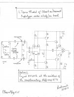
There are 3 different ways ..
To inject balanced full wave analog pulses [[BFWAPs] in a Class AB amp so as to transform it to a Class A on Demand [CAOD] amp. The attached schematic is an LTspice model of the prototype which is on the bench, and shows the first approach to do so. BTW, this model is fully commensurate with the operation of the prototype.
1. BFWAPs are injected at the joint emitter nodes of the front end complementary BJT diff amps.
2. Each pair [NPN and PNP] operates as Common Base amplifiers of the BFWAPs.
3. Their outputs [across R1 and R2] are further presented to the last voltage amps [Q5 and Q6] such that their outputs at their collectors adjust in a dynamic and balanced manner the bias voltage across R5.
4. This balanced and dynamic bias voltage propagates across the common collector BJTs all the way to the power output node. A resultant voltage null [no power output to the load] exists at this node because the BFWAPs are bipolar; meaning they are of equal absolute amplitude and are 180 degrees out of phase.
This LTspice model can be made to run all the way to FFT, and % THD as follows:
1. Convert the frequency of the voltage generators to 4KHz.
2. Use the appropriate commands which I described in previous models as were taught by DIYer Mooly.
3. The Class AB amp can be assessed only by disabling [cut the wires] the Full Wave Rectifier [FWR] as indicated on the schematic.
4. The performance of CAOD amp can thereafter be compared with that of Class AB by re-connecting the FWR.
5. The extent of "dynamic bias enhancement" is readily adjustable by simultaneously manipulating the voltage of the FWR generators or by tweaking R12 and R13 [0.6 Ohms] up or down in value.
6. I view the consequence of this adjustment [by example] across the 0.05 Ohm sense and load resistor of the power PNP.
7. The difference in the shape of the signals is clear. Other differences in the amplitude of the signals was explained in previous posts. All indicate and show that the power output BJTs were denied cut-off which is the technical objective.
Next up is the second method to inject BFWAPs into a Class AB amp.
Best regards.
Attachments
Last edited:
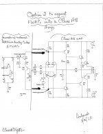
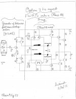
The left image shows an LTspice model schematic of a Class A on Demand [CAOD] power amp utilizing a second and different option to infuse it with Balanced Full Wave Analog Pulses [BFWAPs]. This model schematic was not assembled into a prototype. It is the proverbial cart before the horse. Note the following:
1. It is conventional wisdom and practice to operate the front end diff amps by using constant current sources. In this case they are successfully simulated with the 2.2 K resistors and their associated batteries.
2. The BFWAPs are injected at the collectors of the complementary non-inverting BJTs of the diff amps by using the circuit to the left of the hand-drawn perpendicular line separating it from the Class AB under renovation.
3. The BFWAPs propagate from this point on to the power output stage as described for option 1 in the previous post.
The right image shows an LTspice model schematic of a CAOD utilizing a third and different option to infuse BFWAPs in the Class AB power amp under rennovation. It was not assembled into a physical prototype. Note the following:
1. The generator circuit to the left of the hand-drawn perpendicular line injects its BFWAPs across the bias resistor [of the power output stage] directly; thus totally bypassing the last voltage amplifiers feeding the same bias resistor.
2. The value of this bias resistor was decreased in value to accommodate this approach.
Both LTspice model can be made to run [I confirmed it] all the way to FFTs and % THD independently for Class AB [the parent] and for CAOD [offspring] by using the guidelines [commands from Mooly] of the previous posts.
The appropriate BJTs in the 3 aforementioned flavors of CAOD can be cascoded where/if desired. For example, in the front end diff amps and the last voltage amplifiers. These approaches to making CAODs are not restrictive.
Got two more LTspice model schematics to present; just to broaden this picture. After this I'll discuss thermal management.
Best regards
Attachments
An interesting review article....
of Krell Solo 375 Mono Block power amp by Brent Butterworth in hometheaterreview.com. Krell uses iBias Technology in this amp's Class A output stage in which the bias of its semiconductors is continuously adjusted so as to keep them in this Class A. This practice by Krell of its iBias exemplifies that the dynamic adjustment of bias current in the output stage to maintain Class A operation is alive, well, valuable for audio high fidelity, and hopefully profitable to Krell.
of Krell Solo 375 Mono Block power amp by Brent Butterworth in hometheaterreview.com. Krell uses iBias Technology in this amp's Class A output stage in which the bias of its semiconductors is continuously adjusted so as to keep them in this Class A. This practice by Krell of its iBias exemplifies that the dynamic adjustment of bias current in the output stage to maintain Class A operation is alive, well, valuable for audio high fidelity, and hopefully profitable to Krell.
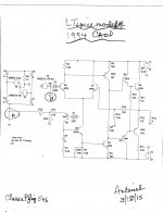
Back in 1994...
I assembled a Class A On Demand [CAOD] prototype using the schematic of the left image. I loved its sound. Fast forward to today to find its LTspice model schematic in the middle image. Let me tell you about the parent Class AB power amp.
1. A front end comprised of an NPN diff amp [Q1, and Q2].
2. The current source circuit [to diff amp] built around Q3 shows a PNP [Q6]/battery [V3 = 3.85 V] instead of a simple resistor to ground.
3. Note the encircled junction labelled A to the far left of the image at R16 = 9 Ohms.
4. This is the point [A] of injecting full wave analog pulses [FWAPs] emanating from the model full wave rectifier above point A.
5. The battery, PNP and R17 =3.3K of the current source define or set the magnitude of the idle currents in the NPN diff amps which propagates further to the power output stage. The voltage of the battery [V3] was temperature sensitive. It decreases as the temperature of the heat sink rises from the dissipation of power output BJTs.
6. Play this game as an example. At the indicated V3 = 3.85V, the idle of each power BJT is 107 mA. At V3 = 3.80V [higher temperature], this model drops the idle current to ~65 mA. There is an actual circuit for this thermal management.
7. The battery [V7 = 0.009V] at point B which is the non-inverting input node of Q2 zeroes the voltage at the power output node. Like a static DC servo.
8. The LTspice schematic of the middle image shows a grounded input [at the hand-drawn circle B], and further enables the injection of FWAPs at point A.
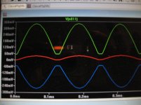
9. I recognized In 1994 that the resultant positive going pulses at the emitter of NPN/Q8 were not equal in absolute magnitude to the negative going FWAPs at the emitter node of PNP/Q10.
10. The right image via LTspice shows this imbalance clearly. The middle trace is the power output voltage across the 4 Ohms dummy load [~50mV] which in a perfectly balanced situation of FWAPs must be zero Volts.
11. This imbalance in the FWAPs has unexpected and interesting consequences on the extent of harmonic distortion and its fine structure.
The next post is dedicated to a comparison [FFT and %THD] between this CAOD and its parent Class AB amps.
Best regards
I assembled a Class A On Demand [CAOD] prototype using the schematic of the left image. I loved its sound. Fast forward to today to find its LTspice model schematic in the middle image. Let me tell you about the parent Class AB power amp.
1. A front end comprised of an NPN diff amp [Q1, and Q2].
2. The current source circuit [to diff amp] built around Q3 shows a PNP [Q6]/battery [V3 = 3.85 V] instead of a simple resistor to ground.
3. Note the encircled junction labelled A to the far left of the image at R16 = 9 Ohms.
4. This is the point [A] of injecting full wave analog pulses [FWAPs] emanating from the model full wave rectifier above point A.
5. The battery, PNP and R17 =3.3K of the current source define or set the magnitude of the idle currents in the NPN diff amps which propagates further to the power output stage. The voltage of the battery [V3] was temperature sensitive. It decreases as the temperature of the heat sink rises from the dissipation of power output BJTs.
6. Play this game as an example. At the indicated V3 = 3.85V, the idle of each power BJT is 107 mA. At V3 = 3.80V [higher temperature], this model drops the idle current to ~65 mA. There is an actual circuit for this thermal management.
7. The battery [V7 = 0.009V] at point B which is the non-inverting input node of Q2 zeroes the voltage at the power output node. Like a static DC servo.
8. The LTspice schematic of the middle image shows a grounded input [at the hand-drawn circle B], and further enables the injection of FWAPs at point A.
9. I recognized In 1994 that the resultant positive going pulses at the emitter of NPN/Q8 were not equal in absolute magnitude to the negative going FWAPs at the emitter node of PNP/Q10.
10. The right image via LTspice shows this imbalance clearly. The middle trace is the power output voltage across the 4 Ohms dummy load [~50mV] which in a perfectly balanced situation of FWAPs must be zero Volts.
11. This imbalance in the FWAPs has unexpected and interesting consequences on the extent of harmonic distortion and its fine structure.
The next post is dedicated to a comparison [FFT and %THD] between this CAOD and its parent Class AB amps.
Best regards
Attachments
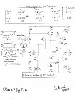
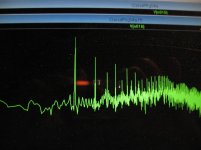
Lots of harmonics...
appearing in the left image from the 1994 vintage CAOD amp [previous post] per its LTspice model in the right image. The top part of the right image tabulates H2, H3 and H4 harmonics for CAOD and its Class AB parent. The performance of Class AB is mostly a clean slate of harmonics. By contrast, this CAOD is a generator of a rich collection of even-order harmonics [H2 and H4]. Tentatively, the cause of this emerging harmonic may be attributed to the imbalance in the bipolar FWAPs [unequal absolute voltage amplitudes] which were presented to the power output BJTs. This outcome of a measurable %THD [0.45] suggests that the unbalanced FWAPs admix [add and subtract] with the symmetrical input AC signal Vi so as to cause asymmetry in its power output signal [in-exact replica].
It was not possible to balance FWAPs with this schematic; though I tried . The circuits of Q3 and Q4 have two confounded parameters, I could either balance the idle conditions [meaning 0 VDC offset at power output] and unbalance FWAPs, or balance FWAPs and simultaneously unbalance the idle conditions.
Fortunately, there is a way out with a beneficial option to control the magnitude of the harmonics to show up in the next post.
Best regards
Attachments
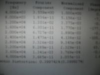
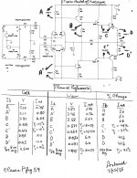
Exercising control over harmonics..
in the left LTspice model schematic which is a modification of that shown in the previous post. In it, the positive and negative going FWAPs were separated at resistors R21 and R18 [encircled]. This gave control over their relative absolute voltage amplitude. The table above the model schematic shows the normalized harmonic distortion; with focus on their phase. In the table the value of R21 was fixed at 1 Ohm, and the value of R18 varied between 1 and 1.55 Ohm. Note:
1. At R18 = 1.25 Ohms, I was able to balance the positive and negative FWAPs and get a minimum THD of 0.06%.
2. At R18 = 1 Ohm, THD [0.76%] was more like found/given in the previous post; meaning the positive FWAPs at the power NPN emitter were larger in absolute amplitude than the negative going FWAPs at the emitter of power PNP.
3. At R18 =1.55 Ohms, the resultant THD [0.76%] emanated from the negative going FWAPs being made larger in absolute magnitude than the positive FWAPs.
4. The right image shows this new state taken at a frequency of 60 Hz; absent an AC input signal Vi..
5. The absolute magnitude of %THD is further tweaked by adjusting the value of the voltage generators in the full wave rectifier at a fixed AC input signal Vi. Or adjusting the values of R18 and R21 in the same proportion while holding the voltage generators of FWAPs and the AC input Vi constant.
There is one more LTspice model schematic in this series. It will show an absolute balance in FWAPs at the emitters of the power BJTs, and thus enable a resultant very low %THD.
Attachments
The left image shows shows the LTspice model schematic of the 1994-style CAOD which has an impressive low THD equal to 0.00025%; namely identical to that of its Class AB parent. Note the following:
1. The generator of precision, and balanced full wave analog pulses [PBFWAPs] to the left of the hand-drawn perpendicular line. Precision was enabled by forward biasing the diodes in the bridge rectifier.
2. The generator pushes its PBFWAPs across the bias resistor [R7 = 275 Ohms] of the indicated parent Class AB amp.
3. The two batteries V7 and V11 which are highlighted with arrows are made to be temperature dependent, either one or both. As the temp of the heat sink rises due to the dissipation of the mounted power BJTs, their voltage drops such that the resultant voltage drop across the bias resistor R7 decreases because the current contribution of their circuits decreases. A mechanism which is different from the shunt regulator in lieu of R7 in a classical class AB amp.
The telltale sign of a Class AB [by example] is the voltage drop across the arrow-highlited sense resistor R10 = 0.05 Ohms [at Q10] which is shown in the far right image. The signal in the first 8 milliseconds runs flat at -20 V; meaning an absent voltage drop across this sense resistor which implies that power PNP is off. The peak current attendant to the tall peak was calculated to be equal to 0.94A
The telltale sign of CAOD is the middle image which shows a short peak in the same early 8 milliseconds of operation. The short peak means the power PNP is active by comparison with Class AB parent. The peak current attendant to the short peak is 0.65A. The peak current due to the tall peak was calculated to be 1.57A. Why is this tall peak of CAOD taller than that of Class AB? It is taller peak in CAOD because there is a short peak like the one next to it hiding under it due to full wave stimulation. The algebraic difference between the currents due to the tall and short peaks in CAOD roughly equal the magnitude of the current attendant to the sole tall peak in Class AB.
The analyses of the 1994-vintage CAOD are complete. I hope that you forgive me for "running wild" with LTspice modeling; but it is the tip of this iceberg nonetheless.
I will describe the circuit and operation of the thermal management of the CAOD prototype which is on the bench, and present real data.
Best regards.
Attachments
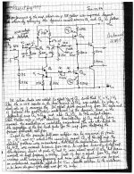
The left image shows the schematic of the bias regulator in association with the generator of precision full wave analog pulses [FWAPs]. This is the exact schematic for its build on the perforated board which I showed in post#109. In operation, the temperature dependent voltage of the bias regulator is summed with positive-going FWAPs [in an Op amp] to feed the emitters of the front end PNP diff amp [at 2.2K node top right of schematic]. This output is simultaneously inverted in a second Op amp to generate a balanced input to the emitters of NPN diff amp.
The BJT of the bias regulator [then TIP31 and now NPN FJ430.. was mounted on the heat sink between the power output BJTs which I showed in post#110. I adjusted its cold or initial VBE [with 20 K pot] at 0.500 V; knowing that this VBE is going to decrease as its temperature rises, and this BJT must stay active and not cutoff for thermal control.
The right image shows a neat LTspice schematic of the prototype which is affected by the bias regulator. Note that I measured DC voltages at the arrow-highlighted nodes under cold [on turn on] and warm conditions of the heat sink. The resultant data are tabulated below this schematic, and are the thermal performance of this Class A On Demand [CAOD] amp. Here are key details of the experiment and analyses:
1. Measured heat sink temperature to equal 15 Celsius with an alcohol thermometer sitting atop it [same as room temp]. Voltage measurements were done within one minute of turn on and define this "cold" status.
2. The measured cold base emitter voltage [VBE] of the power output, and the bias regulator BJTs were associated with this 15 Celsius.
3. VBE of BJT is then used to "quantify or calculate" its junction temperature [Tj]. As the temperature of the junction rises, this VBE declines at an established value of 2 MilliVolts per degree Celsius. Thus I calculated an approximate warm Tj which is important to safeguard the BJTs.
4. CAOD drove the 4 Ohm power output load with a 2 Vp-p for a couple of hours so as to warm up the heat sink, and to establish an approximate thermal steady state.
5. Voltage measurements were taken at this warm status without a power output signal.
Here is the bottom line:
1. Tj of the 3 BJTs rose from 15 [cold] to ~45 Celsius. These calculated values from their VBEs were similar.
2. Idle bias of the power output BJTs decreased from ~100 mA per BJT to 60 mA per BJT [down 40%]. It was over-compensated by the bias regulator.
3. The bias current of the front end diff amps and that flowing through the bias resistor [630 Ohms] declined by ~6 % due to temperature rise. The induced temperature rise [in the bias regulator BJT] decreased its output voltage [left schematic] which further lowered current flow through the 2.2 K emitter resistors to diff amps ......cascading all the way to the power output stage.
The physical size of the heat sink [of this prototype] is small. I use an AC fan to blow on its fins so as make it appear physically larger, and it does lower its warm status to cold [by feel]. This CAOD amp need a bigger heat sink and/or with fan assist so as to safeguard the power out BJTs [SOA] and unacceptable Tjs. This expectation is suggested to other CAODs if assembled by DIYers.
Question: How will this CAOD amp sound if its output stage BJTs idled cold and/or warm at ~2-3 mA instead of 60-100 mA each?. Will report...
I have LTspice model schematics [to show you] for hand-drawn [analog pulse] amp circuits in the very early posts. I am catching up with this intriguing and valuable LTspice tool. The ongoing learning from these models are interesting.
Best regards
Attachments
- Home
- Amplifiers
- Pass Labs
- Class aP amplification