Optimal bias of CAOD amp.
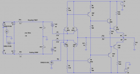
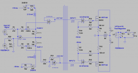
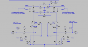
I need two consecutive posts to explain, and elaborate the Title. The left image is the model schematic under study. Its attendant .asc file is attached. This schematic is compliant with the operation of the prototype I have on the bench. Please note the following in this left image. I have adjusted the following values or parameters therein to give this following amp performance:
1. The 2 batteries V3 and V4 [5.65 V] gave an idle current in each power BJT of 105mA.
2. Vin is a 60 Hz signal which has an indicated amplitude of 0.5V. This Vi gives an output voltage ~24 Vp-p across the dummy load of 4 Ohms.
3. The amplitude of FWAPs at the voltage dividers connected to the full wave rectifier [ at emitters of input diff amps] ensured that the power output PNP BJT did not turn off at 24 Vp-p out. This amplitude is the one which fights BJT turn off by advancing current to it.
4. The status of current conduction for the PNP power output BJT was sensed across its 0.05 Ohm collector resistor. One can also sense it across the negative power rail.
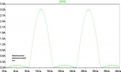
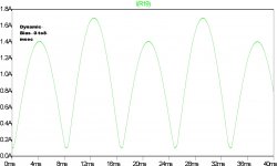
The middle image is the LTspice scope photo of the current flowing through the collector of PNP power output BJT. The short bump in the first 8 milliseconds is the dynamic idle of PNP at full power output into 4 Ohm.
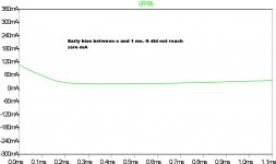
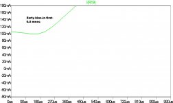
The rightmost image is a magnification of the early bias for the small bump. The current flowing through PNP did not go to zero but hovered about ~20 mA.
One can readily compare the operation of the parent or reference Class AB amp with the above. Disable the feed-line of FWAPs and run the .asc file.
In the next post I will keep the schematic of this post constant and do one single change. I will lower Vin to 0.05V. This will give the full snapshot of the status of bias under dynamic conditions for high, and low power output operation.
Best regards.
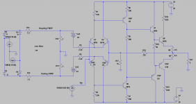
I need two consecutive posts to explain, and elaborate the Title. The left image is the model schematic under study. Its attendant .asc file is attached. This schematic is compliant with the operation of the prototype I have on the bench. Please note the following in this left image. I have adjusted the following values or parameters therein to give this following amp performance:
1. The 2 batteries V3 and V4 [5.65 V] gave an idle current in each power BJT of 105mA.
2. Vin is a 60 Hz signal which has an indicated amplitude of 0.5V. This Vi gives an output voltage ~24 Vp-p across the dummy load of 4 Ohms.
3. The amplitude of FWAPs at the voltage dividers connected to the full wave rectifier [ at emitters of input diff amps] ensured that the power output PNP BJT did not turn off at 24 Vp-p out. This amplitude is the one which fights BJT turn off by advancing current to it.
4. The status of current conduction for the PNP power output BJT was sensed across its 0.05 Ohm collector resistor. One can also sense it across the negative power rail.
The middle image is the LTspice scope photo of the current flowing through the collector of PNP power output BJT. The short bump in the first 8 milliseconds is the dynamic idle of PNP at full power output into 4 Ohm.
The rightmost image is a magnification of the early bias for the small bump. The current flowing through PNP did not go to zero but hovered about ~20 mA.
One can readily compare the operation of the parent or reference Class AB amp with the above. Disable the feed-line of FWAPs and run the .asc file.
In the next post I will keep the schematic of this post constant and do one single change. I will lower Vin to 0.05V. This will give the full snapshot of the status of bias under dynamic conditions for high, and low power output operation.
Best regards.
Attachments
Part 2 Optimal bias of CAOD
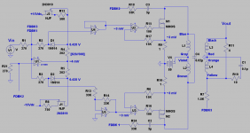
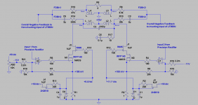
The left image is the same schematic which I already showed in the previous post; except I lowered Vin to 0.05V from 0.5V. This gave a voltage output across the same 4 Ohm load of ~2.4 Vp-p. The attendant .asc file is also attached. Note the following.
1. The middle image from the LTspice scope describes the dynamic bias of PNP power output in the time lapse of 0 to 8 msec. The small bump which I showed in the previous post is a much taller peak; meaning a high dynamic bias current.
2. The difference in the amplitude of the two peaks in the first 16 msecs is the power output current delivered by PNP [0.3 Ap] to the 4 Ohm load .
3. The rightmost LTspice scope photo shows the magnified early dynamic bias of PNP power output. PNP was on and was not inclined to turn off by dropping to zero mA.
Two conclusions emerged from the 2 posts on biasing this amp:
1. The amp chewed up a lot of current at low Vin in the process of delivering a meager output current.
2. Calling this amp Class A On Demand does not describe it properly as the middle image clearly showed. The circuitry of FWAP does not track Vin like designs of past commercial amps.
I hope these past few posts gave a good feel of this other approach to manipulating the bias of the power output stage so as to deter its BJTs from turn off. It is user-adjustable to comply with any preset level of output power in any preset load values.
I got LTspice models to show you for the Analog Pulse [AP] prototype amps I described in detail early in this thread.
Best regards.
Attachments
Look back at older prototypes with LTspice Models
Please find attached LTspice model schematics of Analog Pulse amplifiers which are commensurate [in operation] with the bench prototypes that I reported early in this thread. Their attendant .asc files are attached.
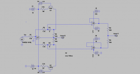
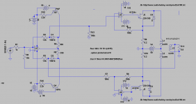
The left image is a model of a Precision Rectifier:
1. PR60.asc file generated this image.
3.The left side is the workhorse precision rectifier.
4.The right side is made of two buffers. Their load resistors splice the Analog Pulses [entering their +inputs] and reconstitute the input AC signal so as to assess it for % THD; which is a measure of the accuracy of the Precision Rectification. It was precise and accurate too.
5. The content of %THD of the reconstituted AC signal is exclusively Odd-Order Harmonics. Ditto at the output of the Precision Rectifier Op Amp; but its % THD was higher; presumably due [or a manifestation] to absorbing the switching aberrations of the diodes.
There is a suggestion that Rectification and odd-order harmonics are correlated.
The right image is model schematic [application] of a Current Source AP power amp which was discussed earlier in detail.
1. The second .asc file generated it
2. The left and middle part of the image was described above.
3. The rightmost part of the image is the power output stage which idles at ~120 mA per branch.
4. Note the nodes which I highlighted. They reconstituted the input AC signal at the output of the Op Amp buffers, and [after amplification] reconstituted at the two dummy 8 Ohm loads. This was done to assess % THD.
5. The Run Commands will take its .asc file to FFT and % THD at the selected output node.
The content of % THD at the reconstituted power output nodes was higher than that at the preceding output of Op Amp buffers. Both were exclusively rich in odd-order harmonics. The power output stage appeared to amplify the odd-order harmonics from the Op Amps, and further augmented their amplitude by generation within.
I'll search my notes for other unreported schematics, and present them as LTspice models.
I do hope that I have done this topic justice in modelling and practical prototyping.
Best regards.
Please find attached LTspice model schematics of Analog Pulse amplifiers which are commensurate [in operation] with the bench prototypes that I reported early in this thread. Their attendant .asc files are attached.
The left image is a model of a Precision Rectifier:
1. PR60.asc file generated this image.
3.The left side is the workhorse precision rectifier.
4.The right side is made of two buffers. Their load resistors splice the Analog Pulses [entering their +inputs] and reconstitute the input AC signal so as to assess it for % THD; which is a measure of the accuracy of the Precision Rectification. It was precise and accurate too.
5. The content of %THD of the reconstituted AC signal is exclusively Odd-Order Harmonics. Ditto at the output of the Precision Rectifier Op Amp; but its % THD was higher; presumably due [or a manifestation] to absorbing the switching aberrations of the diodes.
There is a suggestion that Rectification and odd-order harmonics are correlated.
The right image is model schematic [application] of a Current Source AP power amp which was discussed earlier in detail.
1. The second .asc file generated it
2. The left and middle part of the image was described above.
3. The rightmost part of the image is the power output stage which idles at ~120 mA per branch.
4. Note the nodes which I highlighted. They reconstituted the input AC signal at the output of the Op Amp buffers, and [after amplification] reconstituted at the two dummy 8 Ohm loads. This was done to assess % THD.
5. The Run Commands will take its .asc file to FFT and % THD at the selected output node.
The content of % THD at the reconstituted power output nodes was higher than that at the preceding output of Op Amp buffers. Both were exclusively rich in odd-order harmonics. The power output stage appeared to amplify the odd-order harmonics from the Op Amps, and further augmented their amplitude by generation within.
I'll search my notes for other unreported schematics, and present them as LTspice models.
I do hope that I have done this topic justice in modelling and practical prototyping.
Best regards.
Attachments
The image shows an LTspice schematic of a bench prototype which I assembled in the mid 1990's. Its .asc files runs. It uses two complementary BJTs to simultaneously rectify and amplify the input AC signal to the Op Amp. The resultant positive and negative-going Analog Pulses are offered to complementary Darlingtons [then TIP 120 and TIP 125] which are connected in a common-emitter-opposed collector configuration. Overall negative feedback is returned to the inverting port of the Op Amp. Complementary Mosfets were also used instead of the Darlingtons. I still have these two output stages on their heat sinks.
Like some of the previous amplifiers based on Analog Pulse techniques, the harmonic structure of this amp is rich in 3rd harmonic. Furthermore, the output stage BJTs does not turn off by intentional objective.
Best regards.
Like some of the previous amplifiers based on Analog Pulse techniques, the harmonic structure of this amp is rich in 3rd harmonic. Furthermore, the output stage BJTs does not turn off by intentional objective.
Best regards.
Attachments
The image dates to 1998. It shows a simplified schematic of a transformer-coupled push-pull analog pulse amplifier [APA]. This simple prototype had the basic components of a typical Class AB or Class B power output stage. In operation, the same polarity bjts [TIP120 NPN by example ] of this type of an established Class AB or Class B amp simultaneously rectify the input AC signal and amplify its resultant half-wave [or analog] pulses. The power output transformer then splices these [discrete] pulses back into a harmonic power output AC signal. By comparison with this typical Class AB/B power amp, the operation of APA is different, and may be understood as the following two step operation. It is a different means to the same end...
1. A first step rectification of the input AC signal to generate Analog [half wave rectified] Pulses in a dedicated [Precision Rectifier] circuit which precedes, and is independent of the power output NPNs.
2. This solo precision rectifier gives independent Positive and Negative-going pulses as its desired signal [pulse] outputs.
3. The positive-going pulses are presented to one bjt for power amplification. 4. The other negative-going pulses are first inverted and then presented to the second bjt for power amplification at a time which comes later as defined by the original AC signal.
Separating rectification from amplification in APA is expected to give the experimenter added degrees of freedom to tweak, design ...etc. The penalty is clearly an added circuit complexity.
I will will show in the next two posts two LTspice models of the prototype in image. One model uses NPN Darlingtons, and the second uses SIT; which by extension is expected to model vacuum tubes.
Best regards.
Attachments
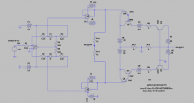
The image is an LTspice model schematic of a transformer-coupled push-pull analog pulse amp [APA] using NPN power output Darlingtons. Its .asc file is also shown with commands to run it to fft, and %THD per the teachings of DIYer Mooly.
The circuit of Op Amp U1 to the left of the image is the Precision Rectifier [PR].
1. I used 1N914 fast switching diodes.
2. LTspice said that an optimum 30uA bias through each diode gave the lowest %THD in this PR circuit which was predominantly odd-order harmonics.
3. A resultant voltage drop of ~+/-45mVDC appeared across the 1.5K resistors [30uA times 1.5K] terminating at the inverting input of the U1 [virtual ground]. This small DC offset is needed and a plus to bias the power output stage.
4. LT has a rich collection of Op Amps. Its generic universal OA did a great job in this application.
The middle part of the schematic shows the power NPN Darlingtons connected inside the feedback loops of their respective buffer Op Amps. This arrangement makes "perfect" BJTs via error correction, and further presents the 45 mVDC offset from the PR to appear across their emitter resistors so as to generate their idle current. Note that the lower Op Amp inverted the negative-going analog pulses prior to presentation to the lower NPN as I mentioned in the previous post.
The right part of the schematic shows a concept power output transformer. Thanks to Gabino Alonso of Linear Technology for his clear YouTube video in which he taught making a "transformer" in LTspice. Overall negative feedback is returned from the transformer's secondary winding [loaded] to the inverting input of the PR's Op Amp.
Noteworthy is that the value of the BJTs' emitter resistors controls both their idle current, and the gain of their output stage. One also can decrease the value of the resistor at the input of the PR inverting port so as to increase the voltage gain of this PR circuit. The calculation of open and closed loop voltage gains are thus rendered straightforward.
The predominant harmonic profile of this amp is odd-order. The above verbiage sets the stage for the following post using SIT instead of BJT in the output stage.
Best regards.
Attachments

A closing post
The image shows an LTspice model schematic of a transformer-coupled push-pull analog pulse amp utilizing 2SK180 in its power output stage. Its tracking .asc file is also shown.
Thanks to M. Rothacher for his clear YouTube video in which he taught "assembling his " L'Amp.. in LTspice, and showing how to fetch or import this SIT and its "specs" into the model by using the .lib directive.
Noteworthy are the following:
1. This schematic has the same format as the one in the previous post using BJTs.
2. 2SK180 is inside the feedback loop of its attendant Op Amp.
3. This arrangement is valuable. The Op Amp gives the gate of 2SK180 a negative bias of ~minus 9.2Vdc, and an attendant idle current via the 45mVdc across its source resistor to ground. This bias voltage 0f -9.2Vdc is within the voltage output capability of most Op Amps [shown with +/-18Vdc power rails].
4. The %THD profile of this amp has a dominant 2nd order harmonic.
5. In operation, the positive going analog pulses move the idle gate voltage of -9.2Vdc in the direction of zero volts; meaning they sequentially increase conduction of current in the SITs.
One may wish to extrapolate this model to vacuum tubes. Op Amps which are labelled as "high voltage" will be required to generate at their output the needed negative grid bias; which may easily exceed -15Vdc. Another interesting device to use in this model is the solid state Pentode which was created by Dr. Mazzola [semisouthfan].
Best regards.
A practical amplifier
Hello. The last 4 posts described the simplest approach to practice an analog pulse amplifier. Please take some time to review them. The schematic attached in this post belongs to an experimental prototype which I have assembled to demonstrate feasibility. Please note the following:
1. The notes in the upper left corner which detail the identity of components, etc.
2. The layout may be considered to be like that of a push-pull Class B tube power output stage.
3. The gates of the N-Mosfets are presented with only positive-going pulses.
4. The pulses alternate sequentially between one gate and the other.
5. The pulses emanate from a preceding line-level stage which is a precision half wave rectifier. I'll show in a separate post its detailed schematic.
6. Each Mosfet has an idle current of 100 mA. Neither Mosfet turn off [idle= 0 mA] during the processing of pulses.
7. Not shown is a provision for overall negative feedback. It emanates from the secondary winding of the transformer like in standard designs.
8. The toroid power output transformer of amp is a standard AC power-line type.
Best regards
Attachments
Photos of the experimental amp
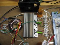
The attached photos show the building blocks of IRFP140Amp under study.
1. The far left photo is the amp's power supply. It is a variac-controlled dual power supply [up to plus 55 Vdc and minus 55 Vdc] of a spent Radio Shack receiver originally rated to deliver 75 W/Ch into 8 Ohms. It is hefty.
2. The AC cord of the receiver is connected to the output of the variac.
3. The negative rail of this power supply is made to be the common or ground to the amp, and the positive rail is the +80 Vdc that is shown on the schematic of the past post.
4. I used a maximum voltage of 80 Vdc for my safety, and to protect IRFP140 which has a max Vds of 100 Vdc.
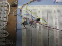
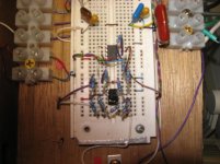
5. The photo next to the power supply is the precision half wave rectifier. The bottom Op Amp [LF356] receives an input audio signal, and also receives a feedback signal from the secondary winding of the power output toroid transformer.
6. This line-level precision rectifier has 2 outputs and a common. Both outputs are positive-going pulses.
7. The photo to the right of the precision rectifier is the driver [labeled OPA2134] to the Mosfets. Its 2 inputs 1 and 2 [in schematic] are the outputs of the precision rectifier.
8. N.B. The top Op Amp in the photo of the precision rectifier is also OPA2134 used as a dual buffer. It can be used as the driver to the Mosfets, and thus eliminate one dual Op Amp from this amp. This approach then defaults to the two schematics that are shown in the spice models.
9. The far right photo is the power output stage. The 1 Ohm Mosfet-source resistors are in the prescription containers.
10 Each Mosfet idles at 8W. I helped the dissipation of the pair with a variac-controlled AC fan.
I hope the past two posts give you a broad picture of this amplifier. I owe you first a schematic of the precision rectifier as used for accuracy. I'll then show objective performance as needed.
Best regards.
The attached photos show the building blocks of IRFP140Amp under study.
1. The far left photo is the amp's power supply. It is a variac-controlled dual power supply [up to plus 55 Vdc and minus 55 Vdc] of a spent Radio Shack receiver originally rated to deliver 75 W/Ch into 8 Ohms. It is hefty.
2. The AC cord of the receiver is connected to the output of the variac.
3. The negative rail of this power supply is made to be the common or ground to the amp, and the positive rail is the +80 Vdc that is shown on the schematic of the past post.
4. I used a maximum voltage of 80 Vdc for my safety, and to protect IRFP140 which has a max Vds of 100 Vdc.
5. The photo next to the power supply is the precision half wave rectifier. The bottom Op Amp [LF356] receives an input audio signal, and also receives a feedback signal from the secondary winding of the power output toroid transformer.
6. This line-level precision rectifier has 2 outputs and a common. Both outputs are positive-going pulses.
7. The photo to the right of the precision rectifier is the driver [labeled OPA2134] to the Mosfets. Its 2 inputs 1 and 2 [in schematic] are the outputs of the precision rectifier.
8. N.B. The top Op Amp in the photo of the precision rectifier is also OPA2134 used as a dual buffer. It can be used as the driver to the Mosfets, and thus eliminate one dual Op Amp from this amp. This approach then defaults to the two schematics that are shown in the spice models.
9. The far right photo is the power output stage. The 1 Ohm Mosfet-source resistors are in the prescription containers.
10 Each Mosfet idles at 8W. I helped the dissipation of the pair with a variac-controlled AC fan.
I hope the past two posts give you a broad picture of this amplifier. I owe you first a schematic of the precision rectifier as used for accuracy. I'll then show objective performance as needed.
Best regards.
Attachments
PowerAmpIRFP140
The schematic of the complete amplifier [less PSU] is attached. Please note:
1. The schematic of the precision rectifier is to the left of the 5 lines in the middle of the view.
2. Overall negative feedback [ONF] emanates from the secondary winding of the power output transformer, and terminates at the non-inverting input of the front-end LF356N.
3. The input AC signal and the feedback signal are in phase.
4. Another option for ONF is also available. It terminates instead at the inverting input of LF356N.
5. I've added a Zobel across the secondary winding of the transformer.
Next up are objective measurements.
Attachments
Amp's objective performance
The attached schematic is a simplified version of the complete one I showed in the previous post. I show in it the key circuit points I used to measure voltages so as to determine Open and Closed loop gains. Please note the following:
1. The two secondary windings of the power transformer are connected in series, instead of parallel as I showed in the previous post. The Zobel [not shown] lowers high frequency noise
2. The text in the upper and left corners which explains, and shows the gain calculations.
3. The circuit has two overall negative feedback loops terminating at both inputs of LF356N precision rectifier.
4. Negative feedback from the primary winding of the power output transformer to the inverting input of LF356N is highly effective to cleanup the wrinkled look of the AC signal at both primary windings at 10KHz. It also decreased open loop gain at both primary windings.
5. Negative feedback from the secondary power output winding of the transformer to the non-inverting input of LF356N was effective also in decreasing overall loop gain.
6. I do not show phase dots on the transformers's windings; because....
7. For feedback to the non-inverting port of LF356N, the correct primary winding cleans up the AC signal while connection to the other one causes oscillation.
8. Negative feedback from one secondary winding to the non-inverting port of of LF356N decreases gain, while the alternate connection to the other one increases gain instead.
9. I'll show phase dots and the colors associated with the winding of the transformer in the next post.
Next I 'll raise the rail voltage to a maximum of +80V and determine the minimum closed loop gain and the maximum available power across 4 Ohms. I am listening to the amp. The base is a bit soft and the high end is clean and highly detailed. Easy to listen to. More on this forthcoming.
Attachments

The intent of this design is to mimic a Class B vacuum tube power amp. Its schematic is attached. It has the following improvements over the one I showed previously, and gave a better and efficient overall performance:
1. Each N-Mosfet idles at ~3 mA. Vgs was ~3,5 Vdc. I got rid of the 2.2 MegOhm resistors in the previous schematic [see drivers of Mosfets at the inverting inputs of OAs] which then allowed each Mosfet to idle at 100 mA.
2. The shunt capacitor which is equal to 0.02 uF across the primary windings of the output transformer is needed for a visually-lowest distortion [scope] of a 10KHz sine signal [60 Vp-p, at each primary] before overall negative feedback is applied.
3. Three independent sources for overall negative feedback were identified and used.
4. FDBK1 and FDBK2 emanate from the primary transformer windings and respectively terminate at the inverting and the non-inverting inputs of LF356N which is the precision rectifier. Both feedback inputs clean up the AC signal [scope]; especially at the challenging 10KHz and lower open loop gain.
5. FDBK3 emanates from the secondary transformer winding and terminates at the inverting input of of LF356N. It further lowers closed loop gain such that this new voltage gain is ~one fourth the open loop gain, The extent of of this collective 3-prong feedback [divide by four gain reduction] is believed to be effective in terms of error correction in amplifiers.
Here are objective results:
1. Open loop gain =17 at the secondary output winding across 4 Ohms/80 W. The maximum un-clipped AC voltage at each primary winding was 60 Vp-p at 10 KHz.
2. Closed loop gain= 4 with the 3 feedback pathways enabled.
3. A maximum voltage output of 10-12 Vp-p across 4 Ohms in the frequency range of 100Hz to 10KHz.
Subjectively, I like the sound of this amp. It is clean and detailed [the highs] when driving a 2-way bookshelf loudspeaker [4 Ohms, A/D/S L300C]. Next up will be to use a 3-way [6 Ohms A/D/S L730] loudspeaker, and finally allowing it to drive 2 open-frame 15 inch musical instruments which are connected in parallel [net =4 Ohms]. Details are forthcoming.
N.B. Overall negative feedback to the non-inverting input of LF356N [FDBK2] generated an interesting operational quirk. I' ll show it in the next post and point to the next steps planned for this prototype amp design.
Attachments
I spoke in the above post of an operational quirk when negative feedback was applied to the non-inverting input of precision rectifier LF356N front end Op Amp.
1. The attached right photo is an example of analog pulses observed across the 1 Ohm resistor which is connected to the source lead of either Mosfet. But only under the two conditions of no negative feedback and/or with negative feedback to the inverting input of LF356N [FDBK1 and 3].
2. So, one Mosfet is active during the first left pulse [time = 0 to t] and then idles or is off in the valley during time = t to t1.
3. The second Mosfet did the opposite behavior in the same time frame. It was idle/off during time = 0 to t and was energized with an identical analog pulse during time = t to t1.
4. Points 1-3 describe Class B push pull operation; in this case absent crossover of the devices and its resultant distortion .
5. The left photo is an example of analog pulses across the same 1 Ohm source resistor when FDBK2 was then enabled to the non-inverting input of LF356N.
6. The short pulses are tracked to FDBK2 and the tall pulses are consequent to FDBK1, and 3.
7. This synthesis of pulses is readily explained by noting that LF356N operates as a Diff Amp and as Precision Rectifier.
8. The consequence of this string of pulses on operation are best understood in points 9 and 10 which shows them as a function of time. T and S denote tall and short pulses. The axis of time is read from left to right.
09. LMosfet:TSTSTSTSTSTSTSTSTSTST
10. RMosfet:STSTSTSTSTSTSTSTSTSTS
11. The above schemes in 9 and 10 show that each Mosfet is continually active in the time frame t=0 to t1; except instantaneously at the zero crossing of the parent AC input signal. One Mosfet amplifies a Tall pulse while the other Mosfet simultaneously amplifies a Short pulse.
12. The primary windings of the power output transformer process two simultaneous pulses which are in-phase but unequal in amplitude.
13. The primary windings subtracts the amplitude of the two pulses and behaves as a "differencing" device.
14. Point 13 is the mechanism for gain reduction due to the 3 prong overall negative feedback.
I'll stop for now and follow with an addendum post on a practical application of the 3 prong feedback.
Attachments
This prototype enabled me to relate its subjective with its objective performance. The additional purpose is to mate it with a loudspeaker I already have. For example the two 15 inch musical instruments; reputed to be full range and connected in this experiment in parallel [4 Ohms load].
1. An idle bias of 100mA instead of 3 mA for each Mosfet sounded great; absent any negative feedback. This amp [100 mA idle] appeared to behave as a current source with a bright high end. This system was displeasing at the low 3 mA idle status; scratchy. The scope trace of proxy sine wave signals predicted and confirmed it. Sharp edges and wrinkles on them.
2. This amp-speaker system sounded great and pleasing when using an idle of 3 mA per each Mosfet, and a negative feedack from the primary winding to the inverting input of LF356N [FDBK1]. Sounded like a current source amp driving a full range loudspeaker which I was well familiar with its performance.
3. More negative feedback [FDBK1 and FDBK3] changed the subjective performance regarding the balance of the audio spectrum. Fully satisfactory; but less pleasing than the case in point 2. Maybe the amp moved a bit away from current source towards voltage source due to the increased feedback.
4. With all 3 feedback loops engaged, the subjective performance of the system changed again. Fully satisfactory; but I liked best the performance of the system described in point 2.
5. I hope that you got a feel for mating a loudspeaker with this amp. And the practice of relating the subjective [listening] with objective performance by separately using the quality of AC sine signals [as proxy to music] on the scope [and/or other device] with negative feedback and its extent etc.
The knowledge I gained from this prototype will enable me to experiment with other power output FETs; namely SONY's 2SJ28, and SemiSouth's R085. Both are normally-on [depletion] unlike the IRFP140's I am using. The prototype using 2SJ28 will attempt to mimic a triode power amp.
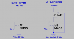
Power Amp with SJDP120R085
SJDP120R085 [R085 for short] is a depletion mode or a normally-on power Junction FET. It was used as described below in the parent schematic shown in post #153 so as to improve its performance; which I am glad to report that it did.
The left schematic shows that R085 was used to cascode IRFP140 of the base amp.
1. A value equal to -5 Vdc for Vgs of R085 turned it off.
2. This value is similar to that declared [by SemiSouth] in the-performance sheet of R085.
3. The Vsg of R085 of 5 Vdc is also Vds for IRFP140. This baseline Vds for IRFP140 is readily increased by shifting the voltage of R085's gate to any desired higher value.
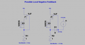
The right schematic shows two additional and possible modes of operation which can adjust for Vds of IRFP140, and also provide a potential avenue for local negative feedback.
The far right topology in the right schematic was used to assemble this newer prototype. I have not yet enabled this local negative it depicts.
In the next post I'll show the new schematic and the build.
SJDP120R085 [R085 for short] is a depletion mode or a normally-on power Junction FET. It was used as described below in the parent schematic shown in post #153 so as to improve its performance; which I am glad to report that it did.
The left schematic shows that R085 was used to cascode IRFP140 of the base amp.
1. A value equal to -5 Vdc for Vgs of R085 turned it off.
2. This value is similar to that declared [by SemiSouth] in the-performance sheet of R085.
3. The Vsg of R085 of 5 Vdc is also Vds for IRFP140. This baseline Vds for IRFP140 is readily increased by shifting the voltage of R085's gate to any desired higher value.
The right schematic shows two additional and possible modes of operation which can adjust for Vds of IRFP140, and also provide a potential avenue for local negative feedback.
The far right topology in the right schematic was used to assemble this newer prototype. I have not yet enabled this local negative it depicts.
In the next post I'll show the new schematic and the build.
Attachments
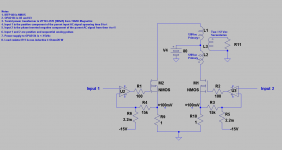
The left image is the schematic for the power output stage of the amp under study. Please note:
1. No local negative feedback was used as mentioned in previous post
2. Each cascode compound idled at 3 mA.
3. The gates of SJDP120R085 were shifted up by ~6 Vdc via the CCS/Zener assembly shown at the bottom right of the schematic. This gave a Vds ~11 Vdc for Mosfets.
4. A provision for overall negative feedback from the primary and secondary windings of power output transformer to the inverting input of LF356N front end. Needs a bit more tweaking.
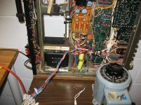
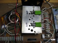
The right photo shows the build with focus on the power output stage:
1. Two heat sinks were used. The top one holds the R085 pair and is bolted with cable ties to the bottom heat sink [hidden from view] onto which are a pair of IRFP140 as was shown earlier in post#150.
2. I took extreme care not to damage the R085s. This device is practically a dead short between its drain and source, and is further priced at $45.
3. Note the small light bulb above the toroid. It was once part of a X-mas light string. The bulb's filament opens at ~120 mA, and was used as a fuse; one in series with the drain of each R085 until I got very comfortable with their safe operation.
4. Still, I speculate that the primary winding of the transformer acts as a choke on power turn-on [I lags V]; and thus delays a current surge through R085. Also, the normally-off IRFP140 in series with the source of R085 adds to it another layer of safety.
This amp is stable against oscillation. It sounded great and pleasing when driving a full-range loudspeaker and a 2-way bookshelf. The system's music was much more detailed than that due to the parent amp using only IRFP140 only. It has a totally different character to it.
I'll tweak and listen some more and report.
1. No local negative feedback was used as mentioned in previous post
2. Each cascode compound idled at 3 mA.
3. The gates of SJDP120R085 were shifted up by ~6 Vdc via the CCS/Zener assembly shown at the bottom right of the schematic. This gave a Vds ~11 Vdc for Mosfets.
4. A provision for overall negative feedback from the primary and secondary windings of power output transformer to the inverting input of LF356N front end. Needs a bit more tweaking.
The right photo shows the build with focus on the power output stage:
1. Two heat sinks were used. The top one holds the R085 pair and is bolted with cable ties to the bottom heat sink [hidden from view] onto which are a pair of IRFP140 as was shown earlier in post#150.
2. I took extreme care not to damage the R085s. This device is practically a dead short between its drain and source, and is further priced at $45.
3. Note the small light bulb above the toroid. It was once part of a X-mas light string. The bulb's filament opens at ~120 mA, and was used as a fuse; one in series with the drain of each R085 until I got very comfortable with their safe operation.
4. Still, I speculate that the primary winding of the transformer acts as a choke on power turn-on [I lags V]; and thus delays a current surge through R085. Also, the normally-off IRFP140 in series with the source of R085 adds to it another layer of safety.
This amp is stable against oscillation. It sounded great and pleasing when driving a full-range loudspeaker and a 2-way bookshelf. The system's music was much more detailed than that due to the parent amp using only IRFP140 only. It has a totally different character to it.
I'll tweak and listen some more and report.
Attachments
PowerAmpR085E
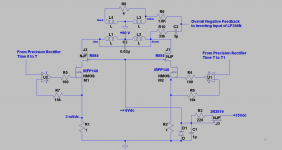
The schematic of the amp's power output stage is attached. The front end Precision Rectifier driving it is the same as was shown in the above posts.
The subjective performance of this amp driving a 3-way loudspeaker [L730] was excellent. It expressed a tight and well defined base which was further coupled with a highly detailed mid-range/high end.
The objective performance follows. Please note first the following circuit changes compared to the previous cascoded amp.
1. Power rail of +100Vdc
2. The voltage gain of each cascode compound was increased from a past 1 to 2.3 from the standard equation: [1+{20K/15K}]=2.3
3.The bias voltage at the gates of R085 was increased asymmetrically as shown in the bottom left and right corners of the schematic [8.4 V, and 11.1 V]
4. This enabled a 15.5 Vdc for Vds of each Mosfet.
5. Four points of overall negative feedback [labelled FDBK1,2,3,4] emanate from the power output transformer; two from the primary and two from the secondary windings.
6. This amp is stable against oscillation with the indicated protocol of feedback used.
Please note the gain relationships when the FDBK1,2,3,4 circuits were enabled.
1. Open loop gain [at secondary winding] driving a 4 Ohm resistor load =42
2. Add FDBK1 and measure gain = 17
3. Add FDBK1 and FDBK3, and measure gain =10
4. Add FDBK1 and FDBK3, and FDBK4 and measure gain = 8.7
5 Add all 4 FDBKs and measure gain= 7.6.
6.The expenditure of 15dB gain or a the equivalent gain reduction by a factor of 5.5 [42 divided by 7.6] is believed to invoke an adequate overall negative feedback and thus reap its expected benefits.
Where to next? Remove the Mosfets, and the level shift voltage circuits to the gates of R085. And thus assemble a plain power output stage comprised of two R085s like I had done earlier with just using the two IRFP140's.
Attachments
Addendum to PowerAmpR085E
The subjective performance of PowerAmpR085E [previous post] driving a pair of 15 inch musical instruments connected in parallel [net Z=4 Ohms] was also excellent in term of definition and spectral balance from top to bottom. The sound of this amp was highly detailed when driving my diy helmet loudspeaker [Z=4 Ohm]. A description of all of the loudspeakers I used to assess the amp's performance have been discussed in past posts.
The overall negative feedback network in this amp was generated by trial and error as I eye-balled on the scope the quality of the power output AC signals, [100 Hz, 1 KHz, and 10 KHz] on the scope. But here's an interesting connection from the gain data which I already presented in the previous post:
1. The sum contribution of overall negative feedback [ONF] to the non inverting port of LF356N front end was calculated to be -9.1 dB
2. The sum contribution of ONF to the inverting port of LF356N was calculated to be -4.7 dB.
3. This begged the question what if I adjusted the relative contribution of ONF to LF356N such that it was mostly sent to either the inverting or non-inverting port of LF356N. A half and half contribution and others were also at hand.
The attached schematic shows a modified ONF circuit but with no other changes to the base PowerAmpR085E [previous post]. It fed mostly the inverting port of LF356N; namely calculated equal to -12.5 dB due to inverting and -0.7 dB due to non-inverting connections. Must also note the following improvement:
1. The Zobel which was present at the secondary winding of the transformer is now on the primary side; where it improved the visual performance of AC signals on the scope better than the original 0.02uF across the primary windings.
The subjective performance of this reworked amp [PowerAmpR085EE] was also equally excellent driving the L730 3-way loudspeaker. But it was discernibly different from the parent PowerAmpR085E; which made me move to favor it over that due to the parent.
I thus have a power amp which can have a different subjective performance which is a sole function of the ONF circuit used therein.
Attachments

PowerAmpR085GG
The attached schematic is a final edition of the power amp utilizing SemiSouth JDP120R085 JFETs used therein to mimic that utilizing vacuum tubes. Please note the following minor modifications to the one shown in the previous post:
1. Idle current in each cascode compound was increased to ~100 mA from 3-6 mA shown in past posts. It can be made variable up or down in magnitude.
2. This higher idle bias was enabled as shown by example in Op Amp U2 driving the left cascode compound leg.
3. A 10 K variable resistor [R20] was connected between -15 Vdc and ground. Its wiper generated ~- 11 Vdc which fed a 2.2 MegOhm resistor [R21] that is connected to U2's inverting input.
4. This arrangement put +100 mV across the R1 [1 Ohm] source resistor to IRFP140 [M1].
5. A capacitor [C2 = 0.02uF] was added across the primary windings of the power output transformer. It eliminated a VHF oscillation when the amp drove a loudspeaker; full range or a boxed 2-way.
The 100 mA idle current in each leg of the cascode compound of the power output stage gave a tremendous [visual] improvement in the quality of in-process analog pulses [at the 3 ports of Mosfets], and for the resultant power output AC signal before Overall Negative Feedback was enabled. The subjective performance in the 2-Way L300C loudspeaker was pristine, and detailed from top to bottom.
Two consequences emerged:
1. A barely perceptible hum which was absent at the low idle state.
2. An idle power dissipation for each R085 which is equal to 0.1 A X [70V-15Vds Mosfet] = 5.5 W. I thought it was a bit high for the small heat sink I used to install them. And so I lowered +Vcc from 100 V to 70 V to protect the R085s.
N.B. This relates to this phenomenon I found for R085. One R085 has a zero gate current. The other one has a 13 mA Gate current; which is unaffected or perturbed by my choice of any idle bias. This disparity did not appear to impact subjective or objective performance.
I'll collect my thoughts and post a blurb on the future work aimed at using 2SJ28 in a similar topology.
Attachments
- Home
- Amplifiers
- Pass Labs
- Class aP amplification