Thanks Jan for your honest comments. I apologize [to you] for putting words in your mouth; edited in this formal post but your comment has already appeared in the heads up E-mail to it.Beg to differ - if you read that in my post I have not been clear. I find that this 'pulse' terminology is completely wrong and gives the impression that all you are interested in is sine waves.
The whole issue is separating signal polarities in the pre-stages and combining them again in the output stage.
Without a scope and/or just ears it's pretty much impossible to do a reasonable job in this endeavor. At least get a $250 Rigol scope or something similar and you will look at your circuit with new eyes!
There is a reason that this tread is mostly a monologue.
Jan
I'd love to hear your reason [you did not say], and other reasons from audio DIYers why this thread is a monologue. I hope that I have made myself extra clear regarding this subject matter. I further admit that I am putting the best effort to share this info with y'all.
I have one more experiment to share before this thread can be closed.
I like the quote regarding beliefs at the bottom of your posts.
Beg to differ - if you read that in my post I have not been clear. I find that this 'pulse' terminology is completely wrong and gives the impression that all you are interested in is sine waves.
The whole issue is separating signal polarities in the pre-stages and combining them again in the output stage.
Without a scope and/or just ears it's pretty much impossible to do a reasonable job in this endeavor. At least get a $250 Rigol scope or something similar and you will look at your circuit with new eyes!
There is a reason that this tread is mostly a monologue.
Jan
Hello Jan.
On a lighter note, I have a gut feel that had I sent an article entitled Class aP Amplification for publication in Linear Audio it would have been blown out of the water faster than the speed of sound.
I am glad, and further indebted to diyAudio for the privilege to publish this approach of amplification in this forum. But, I will always be game to write a chapter for publication in books on audio power amplification which you and others offer us, and continue to do so.
Best regards
Application [one of two]
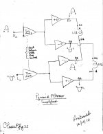
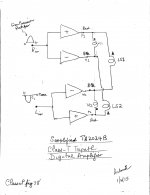
I need two posts to wind down this thread by showing two additional applications of analog pulse amplification. The image pertains to the first application. It depicts a simplified diagram of an automotive stereo amp named Pyramid PB440X which I powered with a 14.4 VDC computer PSU for home use. Noteworthy are the following:
1. Its R and L power outputs bridge the respective loudspeaker loads; meaning they float. This amp is common, and is commonly described as utilizing BTL [bridge-tied-loads]
2. It uses two analog [linear] amps on a single chip [matched] which embody protection against abuse; inadvertent and not.
3. The signal input to Rch is fed a train of positive going pulses from the Precision Rectifier [PR] shown in past threads. The time duration of one pulse is taken as an example to span the time 0 to t seconds.
4. The signal input to Lch is fed a train of negative going pulses from the same PR. The time duration of an example negative pulse is taken to span the later time of t to t1 seconds.
5. The positive and negative pulse pass through the tone amps which share common pots to control volume, bass, and treble.
6. Loudspeaker LS1 is bridged between R+ [0 to t seconds] and L- [t to t1 seconds]. Both power output pulses are positive going, and are sequential in time to generate a bilateral current flow through LS1, and thus reconstruct a harmonic sine wave or music signal. Note the triangle phase marker of LS1.
7. Loudspeaker LS2 is bridged between R- [0 to t seconds], and L+ [t to t1 seconds]. The triangle phase marker on LS2 enables it to operate in phase with LS1. Reverse the phase of LS2 relative to that of LS1 and the bass output disappears; but clean sounding nonetheless.
8. The photo shows LS2 sitting atop of LS1 in a mirror image conformation. One's ear need to be positioned along the line that reaches between the tweeters for an identical arrival time of direct sound from pairs of the mirror image drivers. This pair of bookshelf loudspeakers are Polk Monitor 4B and belong to the Right music channel.
9. There's another pair like it for LCh driven by a second PB440X. This stereo system sounds great. I particularly enjoy the well-crafted song "You'll think of me" by Keith Urban. Whao!. I'll do an Adele...
10. I was surprised that the tone amps were not bothered by [or tolerated] analog pulse signals. The resultant treble-boosted music sounded clean to my hearing.
This app was a stepping stone to this final one which I have not done yet. I will feed music analog pulses through a Class D BTL amp which will be configured like described above.
Best regards
Attachments
One last application
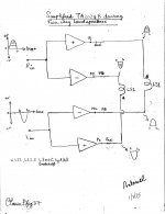
Music signals were precision rectified to generate independent [or electrically separated] positive-going and negative-going Music Analog Pulses [MAP]. These pulses were offered to R and L inputs [respectively] of a Class T digital amplifier which is sold by MCM Electronics [item #50-10145], and made for it by Stellar Labs. The website of MCM shows images of this stereo power amp and gives its performance. The chip therein this power amp is TA2024B made by Tripath.
The left image shows a simplified diagram of the amp' s TA2024B driving a dual voice coil [DVC] subwoofer by utilizing its prescribed BTL connections.
1. An example positive going pulse from the Precision Rectifier [PR] is presented to R input during its active time spanning 0 to t seconds. The R amp drives VC1 such that it pushes its cone out. During the 0 to t seconds, the left channel sat idle; because the negative-going signal was not yet generated to drive it. But, as the cone pushes out, VC2 moves simultaneously in the magnetic field to generate a power signal which is absorbed by the low output impedance of the Left BTL amp
2. The negative-going pulse from PR is presented to L input during its later time spanning t to t1 seconds. Note the triangle phase marker on VC2. The BTL signals pull the cone in. The resultant motion of the cone cause a power signal to develop simultaneously in VC1 which is absorbed by R channel.
3. Most important is to develop a push [by Ramp] and a following pull [by Lamp] motion of the cone so as to splice the MAP signals back to sinusoidal or the like.
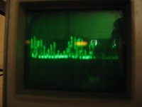
4. The scope photo shows an example of MAP at OutP1 of R amp.
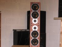
The middle image shows a simplified diagram of TA2024B driving a pair of loudspeakers by utilizing a "crossed BTL" . This is the same approach I described in the previous post using the Pyramid analog BTL amps. The photo shows a picture of a pair of A/D/S L300C loudspeakers [at hand] used for LS1 and LS2 instead of the Polks.
The right image shows the simplified diagram of TA2024B simultaneously driving a DVC enclosed subwoofer, and L300Cs or other pair.
I was surprised these 3 systems [ in images] have a pleasing and detailed sound. I'll buy me a second amp and complete the stereo system.
And that is the way it is.
I hope that y'all have a healthy and prosperous 2015; filled with peace of mind, tranquility and audio DIYs.
Best regards.
Music signals were precision rectified to generate independent [or electrically separated] positive-going and negative-going Music Analog Pulses [MAP]. These pulses were offered to R and L inputs [respectively] of a Class T digital amplifier which is sold by MCM Electronics [item #50-10145], and made for it by Stellar Labs. The website of MCM shows images of this stereo power amp and gives its performance. The chip therein this power amp is TA2024B made by Tripath.
The left image shows a simplified diagram of the amp' s TA2024B driving a dual voice coil [DVC] subwoofer by utilizing its prescribed BTL connections.
1. An example positive going pulse from the Precision Rectifier [PR] is presented to R input during its active time spanning 0 to t seconds. The R amp drives VC1 such that it pushes its cone out. During the 0 to t seconds, the left channel sat idle; because the negative-going signal was not yet generated to drive it. But, as the cone pushes out, VC2 moves simultaneously in the magnetic field to generate a power signal which is absorbed by the low output impedance of the Left BTL amp
2. The negative-going pulse from PR is presented to L input during its later time spanning t to t1 seconds. Note the triangle phase marker on VC2. The BTL signals pull the cone in. The resultant motion of the cone cause a power signal to develop simultaneously in VC1 which is absorbed by R channel.
3. Most important is to develop a push [by Ramp] and a following pull [by Lamp] motion of the cone so as to splice the MAP signals back to sinusoidal or the like.
4. The scope photo shows an example of MAP at OutP1 of R amp.
The middle image shows a simplified diagram of TA2024B driving a pair of loudspeakers by utilizing a "crossed BTL" . This is the same approach I described in the previous post using the Pyramid analog BTL amps. The photo shows a picture of a pair of A/D/S L300C loudspeakers [at hand] used for LS1 and LS2 instead of the Polks.
The right image shows the simplified diagram of TA2024B simultaneously driving a DVC enclosed subwoofer, and L300Cs or other pair.
I was surprised these 3 systems [ in images] have a pleasing and detailed sound. I'll buy me a second amp and complete the stereo system.
And that is the way it is.
I hope that y'all have a healthy and prosperous 2015; filled with peace of mind, tranquility and audio DIYs.
Best regards.
Attachments
Class A on Demand via Analog Pulse Amplification
I look forward to writing a string of posts on this subject. The design and build of this amp preceded the hobby/development work which I have already reported in the past posts. I was fascinated during the 1990's with this broad topic of sliding/dynamic bias for the power output stage BJTs which kept them operating in Class A at all the times. Its technical objectives are like those of any such designs which as an example are well articulated in the Pass patent US 3,995,228. However, I did not know/discern then how well it met these tech and objective requirements.
I have reassembled this voltage source amp for the purpose of telling you its story. I am naming it Class A on Demand instead of Dynamic Class A [DCA] first out of respect to those who came up with the DCA name, and secondly it may not fit well the established or conventional definition of DCA. Its music reproduction sounds great; otherwise I would have buried its forthcoming design blueprints.
Best regards.
Last edited:
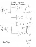
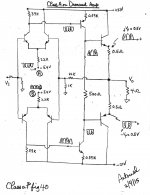
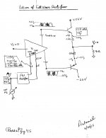
Candidate Class AB amp converted to Class A on Demand.
The image shows a simplified schematic of a ~conventional or basic Class AB power amplifier; which was successfully converted to Class A On Demand [CAOD]. Please note the following which are highly relevant to this conversion, and especially to grasp its concept which is my objective:
1. It is a phase non-inverting voltage source amp of voltage gain [Vo/Vi=23]
2. Each of Q1 and Q2 [output stage BJTs] is actually 3 devices. A Darlington of a pre-driver, a driver, and a high power device on a large heat sink.
3. High power BJTs idle at ~100 mA each.
4.The bias spreading resistor [R =500 Ohms] is between the bases of Q1 and Q2. It is needed instead of the conventional shunt regulator.
5. Points A and B at the emitters of the complementary front end diff amps are the injection ports of analog pulses.
Next up is the schematic of CAOD.
Attachments
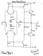
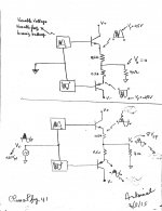
The image shows a simplified schematic of CAOD. Complementary, precision full wave rectified analog pulses [FWAP] are injected at ports A and B. These pulse were generated in a precision full wave rectifier [to be shown] by utilizing music signals, sine waves or others. Note the relative shading of alternate pulses to distinguish their origin of positive or negative going in the sine [for example] parent.
1. Negative going FWAP are presented at point A atop the fixed idle bias generator of -5.4 V.
2. Positive going FWAP of equal absolute magnitude and of inverted phase [as/to those in point 1] are injected at point B atop the fixed idle generator [for diff amp] of +5.4 V.
3. FWAPs then propagate as shown along the amp elements in a symmetrical manner and finally emerge across the emitter resistors [0.5 Ohm] of the high power output BJTs. I show 0.5 V peak as an example at the emitters of Q1 and Q2; which means each BJT passes through it 1 amp peak. It follows that the resultant 2 Ap-p is the CAOD output current which will be made available to the load.
4. The bipolar nature of FWAPs ensures that their resultant voltage at the power output port Vo is/sums to zero volts ; meaning no current flows through the load of 4 Ohms.
5. Note the FWAPs across the bias spreading resistor [500 Ohm]. A conventional shunt regulator instead of this resistor will smooth them out and defeat the intent.
Next up will be an explanation on using this available on demand power output current [trapped in Q1 and Q2] to power the load.
Best regards.
Attachments
Pics of CAOD amp
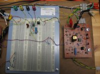
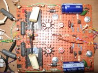
The photo shows the build of the Precision Full Wave Rectifier, and the bias circuit to the complementary diff amps of the power amp. To its left is a solderless proto board. It interfaces this precision rectifier with the Class AB power amp. For example, the bottom left corner shows the 500 Ohm bias spreading resistor.
The AC input signal [for example 100 Hz to 20 KHz from function generator] is offered to the rectifier via the alligator clips. This AC signal is also presented to an OPA2134 buffer [top middle of proto board] which attenuates it prior to presentation to the non-inverting input of the power amp. There is a specific ratio of AC signal for the rectifier to Vi at the input of the power amp.
More pics..
Attachments
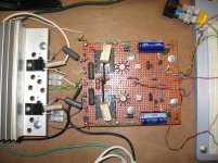
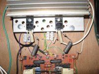
The bottom photo show the build of the Class AB power amp on perforated board. To its right is the interface proto board. At the top right of this photo and on the proto board one sees a compound capacitor [220uF + 1uF+ 0.047uF] which grounds the 1 K resistor at the inverting input. It reduces DC offset at the power output to ~ 2 mV. If this 1 K resistor at inverting port is DC coupled to ground, the DC offset at Vout rises to ~40 mV, and is fully acceptable.
The top right photo shows the output stage of the Class AB amp on heat sink. The BJTs idle at ~ 100 mA each; determined by the value of the bias spreading resistor [500 Ohm] shown earlier on the proto board. The top left photo is a close-up of the Class AB power amp.
I'll copy the schematics of the Precision Rectifier from my notebook and post them as pdf [and backup images]. I'll include the tracking explanation page for each schematic; written in the early 1990s.
Best regards.
Attachments
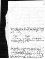
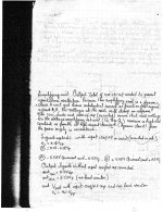
The schematics are in pdf and jpg formats. The schematic of the precision rectifier is in left image and some explanation of it is in the right image; side by side. It pertains to its actual build shown earlier. I bought the referenced book by Graeme in 1976 in Chicago, and still have it.
The bottom schematic and its tracking explanation pertain to a diy thermal regulator practiced then, and not currently. Briefly, as the temperature of the heat sink rises, the circuit lowers the idle bias to the front end of the complementary diff amps of the Class AB amp. Class A on Demand is a heat generator during operation. A large heat sink for the BJTs, or forced air cooling and or the application of this thermal tracker gave a stable amp. I use a fan to cool the heat sink in this CAOD demonstrator.
Two more pages of schematics from my notebook are still needed to complete this picture.
Best regards.
Attachments
Two more schematics
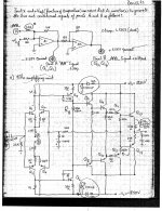
I have schematics [jpg and pdf] which complete the description/picture of Class A On Demand. The total of four schematics thus provide you with a detailed blueprint of its build/assembly.
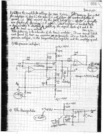
The upper schematic of the left image shows 1/2 of LF353N [A1] summing the full wave analog pulses [FWAP] from the Precision Rectifier with the output of the thermal tracker to generate the idle [-5.58 V] and dynamic bias [negative going FWAP] at point A which is at the emitters of the NPN diff amp in the bottom schematic of the power amp.
The output of the first OP Amp [A1] in the upper schematic is inverted in the second half of LF353N [A2] to generate the idle [+5.58 V] and dynamic bias [positive going FWAP] at point B which is at the emitters of the complementary PNP diff amp in the bottom schematic of the power amp.
The bottom schematic of the power amp was assembled on proto board, and outboard heat sink in 1992. It has morphed since. l'll write a fresh one for the actual build shown earlier.
The past 3 posts are an accurate, and detailed depiction of CAOD under current study. I have more explaining to do in upcoming posts to emphasize this concept.
Best regards.
I have schematics [jpg and pdf] which complete the description/picture of Class A On Demand. The total of four schematics thus provide you with a detailed blueprint of its build/assembly.
The upper schematic of the left image shows 1/2 of LF353N [A1] summing the full wave analog pulses [FWAP] from the Precision Rectifier with the output of the thermal tracker to generate the idle [-5.58 V] and dynamic bias [negative going FWAP] at point A which is at the emitters of the NPN diff amp in the bottom schematic of the power amp.
The output of the first OP Amp [A1] in the upper schematic is inverted in the second half of LF353N [A2] to generate the idle [+5.58 V] and dynamic bias [positive going FWAP] at point B which is at the emitters of the complementary PNP diff amp in the bottom schematic of the power amp.
The bottom schematic of the power amp was assembled on proto board, and outboard heat sink in 1992. It has morphed since. l'll write a fresh one for the actual build shown earlier.
The past 3 posts are an accurate, and detailed depiction of CAOD under current study. I have more explaining to do in upcoming posts to emphasize this concept.
Best regards.
Attachments
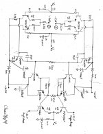
Schematic of amp
Please find attached the schematic of the power amp in pdf and jpg formats. Some aspects of it [e.g. the front end] are in an article in Audio magazine which was a build for a Low TIM amplifier. The power rails to the power output BJTs are high amperage. Both rails droop under load during the operation of CAOD. They are separate from the power rails to the drivers of the power output stage and front end which are lower amperage by comparison.
I will put at select points of this schematic [simplified; e.g. at points A and B, across the bias spreading resistor, Vi, Vo etc.] the levels and shapes of signals which can be AC [sine wave] and/or full wave rectified analog pulses of the same AC signal.
Best regards.
Attachments
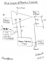
A style to report a study is to start with its conclusion or bottom line; namely its met objective which is the case here.
The attached image is the block diagram of the CAOD. Most important are the shape of the signals and their experimentally determined levels where shown.
1. An AC signal [Vi =100 Hz] is presented to the non-inverting input of the power amp; the schematic of which was already presented in the above post. It is amplified and emerges at its power output port as Vo.
2. The output voltage Vo is equal to 23 Vi and is presented to the dummy 4 Ohm resistor load which is equal to the minimum impedance of the ADS L730 loudspeaker driven by this amp.
3. Vo is further attenuated as shown, and is presented to the Precision Full Wave Rectifier shown in a past post. The outputs of this rectifier are points A and B which carry the idle bias to the front end diff amps onto which are superimposed the Full Wave Analog Pulses [FWAP].
4. By example, the signal conditions [in box] at point A [ditto at point B] are highly relevant. They characterize the operating conditions which render operation as CAOD . The top number [-1.5Vp] is the value from the scope for a negative going 200 Hz FWAP. The number below it [0.441Vac] was measured with a DMM on its AC scale. The next number [-6.37 Vdc] was measured with the same DMM on its DC scale. The last number [-5.4 Vdc] was measured with the same DMM absent FWAP [CAOD at idle].
5. This CAOD was thus adjusted manually to drive a 4 Ohm loudspeaker.
6. This system sounds damn good.
I took my time nailing down the operating conditions at points A and B. I'll tell why in the next post.
Attachments
The image shows the block diagram of CAOD amp which preceded the one in the above post. The focus is on the BJTs of the power output stage, and on the Precision Full Wave Rectifier [FWR]. Please note the idle current through each BJT of 0.1A which maybe a typical value in a Class AB amp.
1. Initially, the level of Vi [100 Hz] at the non-inverting input of the power amp was made equal to zero Vac.
2. A signal from the function generator [level adjustable] was injected at the input of FWR [2.6Vp-p] so as to give a 0.5 Vp of Full Wave Anaolg Pulses [FWAP] across each of the BJT emitter [0.5 Ohm] resistors.
3. It follows that I now know the exact signal levels at the input/outputs [points A and B] of the FWR and the resultant dynamic current in each BJT. I needed these value before [e.g. a priori] I tweaked all of the signal levels in the prototype of the above post.
4. This resultant dynamic current in the power output BJTs [+/-1A peak] may be thought of as a credit advanced by FWR to be exercised when Vi [e.g. a music signal or sine wave ] is next offered to the input of the power amp as follows.
5. As the level of this input signal Vi [0.38 Vp-p from the above post] goes positive in a Class AB amp, there is a point along its climb to its peak value which turns off PNP.
6. By comparison, as the level of the input Vi [0.38 Vp-p] goes positive in CAOD amp, PNP is simultaneously advanced this preset dynamic "credit" current which continually counteracts the action of Vi to turn it off.
7. In the limit of current delivery of NPN [1 A peak] to the load [4 Ohm]; meaning a Vo value of 4 Vpeak across it, PNP is left with only its idle current of 0.1 A. It has successfully spent its allocated credit current, and did not shut off.
8. A similar explanation happens when the level of the input signal Vi goes negative. NPN expends its credit current granted to it by FWR. In the limit of current delivery of PNP [1 A peak; or minus 4 Vp across the 4 Ohm load], NPN has only its idle 0.1 A current flowing through it.
9. Neither BJT was allowed [by the action of FWR] to turn off [due to Vi] during the delivery of 8 Vp-p to the 4 Ohm dummy load. This is the met objective of CAOD
10. I have an experiment to prove the above objective performance which which I'll gladly report in a future post.
I hope that you bear with me for these and more detailed explanations as this CAOD approach [I hope that is understood] has a broader reach into other amp topologies/ designs.
Best regards
Attachments
Addendum to the past 2 posts..
The loudspeaker used [L730] has a minimum and a nominal impedance of 4 and 6 Ohms respectively. Its impedance is like other loudspeakers. It maybe even higher than 4 or 6 Ohms at other frequencies; for example a guessed 16 Ohm impedance at the resonance frequency of its woofer.
The signal levels in this CAOD [2 posts back] were manually adjusted to operate it into 4 Ohms minimum, and at all higher speaker impedance. For example, present the power output voltage Vo of 8 Vp-p [from the above 2 posts] across a 16 instead of the preset 4 Ohm impedance. It follows that the current demand by this 16 Ohm load is only 0.5 Ap-p. Or it is 0.25 A peak per BJT which is less than the preset credit of 1 A peak granted to each BJT by the Full Wave Rectifier. So the load is satisfied, and the remaining unused credit current is still passed in the BJTs. One may view it as a split in the credit current, like 1/4 of it goes in load, and 3/4 of its stays or is dissipated in the BJT. This is a situation which maybe conceptually like any speaker load utilizing 5 W from a 100 W true Class A amp. This Class A amp is loafing..
When the load impedance dips below 4 Ohms, the operation of CAOD goes into Class B. There is not enough credit current to keep the output BJTs from turning off. This lower load impedance maybe fleeting as a function frequency, or sustained.
The CAOD approach differs from past designs which monitor current demand by the load and then react by adjusting the bias current to the output stage so as to satisfy the particular need, and thus keep the BJTs from cutoff which is the objective. I expect this CAOD amp to burn more current in its output BJTs than such past designs. It is a shotgun approach by comparison, because it is is more generous dishing it out counter current in its BJTs than these past designs.
Best regards
The design and operation of this diy Class A on Demand [CAOD] amp is not conventional by any stretch of the imagination. I have this question which kasey197 asked/suggested in an earlier post of this thread. Can LTSPICE or another similar tool simulate, and characterize its objective performance. I hope that an LTSPICE guru like Mooly, lhquam, pr answer this question. Thanks.
Best regards.
Best regards.
Yes LTSPICE will work fine simulating this. Some tricks may be needed for large value caps in the signal pth (dont think that there are any in your schematic}
That will get you in the right ballpark and will also allow others to participate in the development of this amp.
And yes it will get you the objective measurements you will want incl THD, FFT etc etc.
That will get you in the right ballpark and will also allow others to participate in the development of this amp.
And yes it will get you the objective measurements you will want incl THD, FFT etc etc.
Yes LTSPICE will work fine simulating this. Some tricks may be needed for large value caps in the signal pth (dont think that there are any in your schematic}
That will get you in the right ballpark and will also allow others to participate in the development of this amp.
And yes it will get you the objective measurements you will want incl THD, FFT etc etc.
Thanks kasey197 for your reply, and its great news. I am glad to also report that Mike Engelhardt [Tech Service at LTC] gave the identical answer like yours above.
Best regards,
LTSpice'ing ...
An LTspice model for the output stage of a Class A on Demand [CAOD] amp is presented. Here's my explanation of its works:
1. The top middle of the schematic shows diodes [D1-D4] which are a full wave rectifier generating complementary symmetry [bipolar] analog pulses [FWAP].
2. Focus on the positive-going FWAPs which drive NPN. A ditto explanation holds for PNP.
3. The positive FWAPs of the rectifier are presented to a series connected ladder of a resistor [9 Ohm], a 0.95 Vdc battery and terminating in a 0.6 Ohm resistor to common. The battery generates forward bias to NPN. The voltage drop of FWAP across the 0.6 Ohm resistor is the pulse drive to the base of NPN.
4. This arrangement of values for the voltages, resistors etc..was adjusted so as to generate an idle emitter current for either BJT of ~100 mA, and FWAPs of +/- 0.5Vp at their emitters.
5. I believe that [after posting this note], one will be able to run this model and unravel its works. It conforms to the reality of the prototype.
I'll add an input signal Vi to drive the BJTs and a load resistor to this schematic in the following post.
NB. Model did not load.. I'll fool with it.
Best regards
Attachments
Last edited:
- Home
- Amplifiers
- Pass Labs
- Class aP amplification