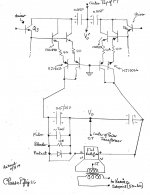
Hi, I am following this thread with curiosity, and I congratulate with you for the initiative to bring forward a new and different idea. The bridge stage you designed is somewhat similar to one of those schematics that I presented a few months ago in this thread:
http://www.diyaudio.com/forums/solid-state/257200-two-new-output-stages-have-you-seen-before.html
with the option of having only two power battery.
Even your circuit could operate with only two batteries (suppressing a pair diagonally), but you may have a different purpose to keep all of them.
I hope that at the end you find some practical benefit (sound). 🙂
Thanks mos57 for your encouraging comments, and your interesting guidance to use 2 batteries instead of 4 in its framework. I'll study your reference thread, paper analyze your suggestion, and gladly report back. I hobbied analog pulse amplification beginning the early 1990s. I am glad that we have stumbled on similar if not identical schematics for an interesting output stage.
You, unlike me endeavors to commercialize your designs [I am thinking your SIT ams]. I have already assembled a bjt-only stereo prototype [demonstrator] which is a best favorite for sound among the standard amplifier designs.
I hope that my continuing flux of info in this thread will not, and did not already interfere with your business practices.
Best regards
You can go on quietly with your ideas and your work.
My bridged schematics had been designed as a possible application of my differential phase splitter that can provide up to four outputs.
If you should find benefit from these sepp/circlotron schemes you can use them without problems. There are no patent or commercial needs at the moment.
Have a nice day, Francesco
Hello Francesco. Thank you for your offer in your above post. I hope to find use for your schematics, and report back.
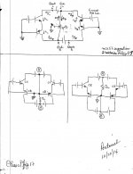
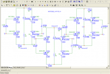
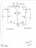
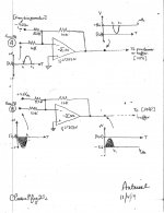
I believe that the top part of the attached image shows the schematic in which you suggested to use 2 instead of 4 power supply batteries. It works on paper, as one follows the alphabetical idle counter current flows in the Left and Right branches. What if the load has a center tap [like a series connected dual voice coil woofer], and I connect it to signal common. Will this action upset idle or other?
The bottom part of the image shows two schematics for the output stage utilizing 4 instead or 2 power supply batteries. My intent to use 2 dual polarity supplies was to build operational flexibility. For example, the left schematic shows that point A [ power output node ] was shorted to signal ground. Thus, the top complementary bjts operate in common collector configuration, and the bottom complementary bjts operate in common base configuration. The schematic on the right shows that I shorted point B[other power out node] to signal ground instead so as to effect a different outcome in performance.
Not shown is a third schematic whereby Zl is connected between points A and B, and with the center point in Zl [if any] connected to signal ground [without detriment to operation], or not.
Best regards.
Attachments
Pictures for a break!
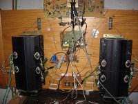
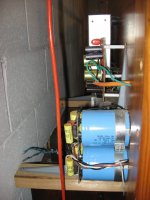
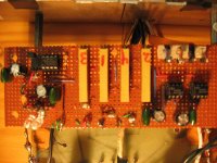
The current source aP stereo amplifier is real and not a pie in the sky. The left photo shows it.
1. Assembled on a solid wood head-board of an unused bed [IKEA]. It is the tan-colored background in photo. It sits upright; meaning I face it.
2. The distance is 26 inches from the left edge of the left tunnel heat-sink to the right edge of the right tunnel heat-sink.
3. The height of each tunnel including an AC fan at its bottom is 14 inches. The width of the tunnel heat-sink is 6.5 inches.
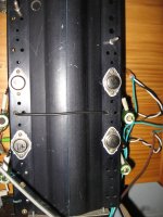
4. The middle to left photo shows a closeup top view of the tunnel heat-sink. Four TO-3 bjts show. Complementary from to to bottom. There are 4 additional TO-3 bjts on its other side.
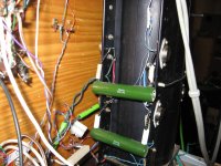
5. The middle to right photo shows a side view of the tunnel heat-sink. The green tubular object is a 4 Ohm 50 W non-inductive resistor. There are 4 such resistors per heat-sink or music channel.
6. The back side of the wood platform has 4 dual power supplies; 2 for the Right and 2 for the Left music channels. They are solely dedicated to their power output stages. A fifth power supply is a regulated +/- 15 V for the Op Amps in Precision Rectifier etc.
7. The right photo shows a side view of the capacitors in the two dual PSUs of the Left channel. The blue containers are 0.1 F/25 V, for the complementary common base part of the output stage. The adjacent dual PSU [above it] has 0.01F caps. Why the mismatch?. Most of the hobby work used only the CC-CB configuration; meaning the spliced sine wave output was derived on the complementary common base part of the output stage.
8. The photos have more detail which will come up in future posts.
9. This prototype is heavy as assembled.
Best regards.
The current source aP stereo amplifier is real and not a pie in the sky. The left photo shows it.
1. Assembled on a solid wood head-board of an unused bed [IKEA]. It is the tan-colored background in photo. It sits upright; meaning I face it.
2. The distance is 26 inches from the left edge of the left tunnel heat-sink to the right edge of the right tunnel heat-sink.
3. The height of each tunnel including an AC fan at its bottom is 14 inches. The width of the tunnel heat-sink is 6.5 inches.
4. The middle to left photo shows a closeup top view of the tunnel heat-sink. Four TO-3 bjts show. Complementary from to to bottom. There are 4 additional TO-3 bjts on its other side.
5. The middle to right photo shows a side view of the tunnel heat-sink. The green tubular object is a 4 Ohm 50 W non-inductive resistor. There are 4 such resistors per heat-sink or music channel.
6. The back side of the wood platform has 4 dual power supplies; 2 for the Right and 2 for the Left music channels. They are solely dedicated to their power output stages. A fifth power supply is a regulated +/- 15 V for the Op Amps in Precision Rectifier etc.
7. The right photo shows a side view of the capacitors in the two dual PSUs of the Left channel. The blue containers are 0.1 F/25 V, for the complementary common base part of the output stage. The adjacent dual PSU [above it] has 0.01F caps. Why the mismatch?. Most of the hobby work used only the CC-CB configuration; meaning the spliced sine wave output was derived on the complementary common base part of the output stage.
8. The photos have more detail which will come up in future posts.
9. This prototype is heavy as assembled.
Best regards.
Attachments
Hello Francesco. Thank you for your offer in your above post. I hope to find use for your schematics, and report back.
I believe that the top part of the attached image shows the schematic in which you suggested to use 2 instead of 4 power supply batteries. It works on paper, as one follows the alphabetical idle counter current flows in the Left and Right branches. What if the load has a center tap [like a series connected dual voice coil woofer], and I connect it to signal common. Will this action upset idle or other?
The bottom part of the image shows two schematics for the output stage utilizing 4 instead or 2 power supply batteries. My intent to use 2 dual polarity supplies was to build operational flexibility. For example, the left schematic shows that point A [ power output node ] was shorted to signal ground. Thus, the top complementary bjts operate in common collector configuration, and the bottom complementary bjts operate in common base configuration. The schematic on the right shows that I shorted point B[other power out node] to signal ground instead so as to effect a different outcome in performance.
Not shown is a third schematic whereby Zl is connected between points A and B, and with the center point in Zl [if any] connected to signal ground [without detriment to operation], or not.
Best regards.
Antoniel to answer your questions I have simulated your circuit of fig.17 with 2 main batteries and the two output loads in series (two speakers) with different points of grounding named A, B, C, D, E, F with the results of the relative current.
Results show that to have no current in the load, if the output branches has a ground point anywhere, the input branches of transistors should not be put to ground and vice versa.
If you grounding on both the input and the output side of the BJT, at the same time, you get dc current on the load (Ground. F).
Attachments
Thank you Francesco for your simulations, and their detailed clarifications. Amplification via aP is expected to work by using your suggested 2 PSUs only; absent grounding the center point in Zl; if present. I can verify experimentally this approach by disconnecting two diagonal "batteries" in both dual PSUs as you mentioned earlier. This is another[ new] flexible mode of operation for aP, which will happen and its performance reported.
Best regards
Best regards
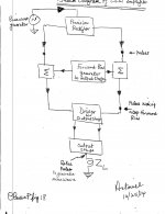
Block diagram of amp.
The attached image shows the block diagram of the Current Source aP Amplifier. Detailed schematics of each block will follow.
1. A sinewave signal is first presented to the Precision Rectifier [PR].
2. PR generates two independent pulse signal outputs; whereby the pulses are sequential in time.
3. An Op-Amp based circuit generates two DC voltages needed to forward bias the complementary bjts downrange its circuit
4. An Op-Amp based amplifier sums or adds the stable DC forward bias voltage with the pulse voltage and generates an output whereby the pulses ride atop the bias voltage.
5. The output of each summing amplifier is presented to a corresponding bjt driver of the output stage bjts.
6. The load Zl zips, or splices, or regenerates a replica of the parent sinusoidal signal which was presented to the input of PR.
The schematics will be presented beginning with PR.
The attached image shows the block diagram of the Current Source aP Amplifier. Detailed schematics of each block will follow.
1. A sinewave signal is first presented to the Precision Rectifier [PR].
2. PR generates two independent pulse signal outputs; whereby the pulses are sequential in time.
3. An Op-Amp based circuit generates two DC voltages needed to forward bias the complementary bjts downrange its circuit
4. An Op-Amp based amplifier sums or adds the stable DC forward bias voltage with the pulse voltage
5. The output of each summing amplifier is presented to a corresponding bjt driver of the output stage bjts.
6. The load Zl zips, or splices, or regenerates a replica of the parent sinusoidal signal which was presented to the input of PR.
The schematics will be presented beginning with PR.
Attachments

Detailed schematic of Precision Rectifier
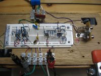
The left image shows a detailed schematic of the Precision Rectifier [PR] currently used in the current source aP amplifier. It is assembled on a protoboard as I showed in a past post. Nothing new therein. Noteworthy to keep in mind are:
1. The relative phase of the pulse signals will be referenced to the sinewave signal input to PR; taken to be absolute.
2. The shaded part of the the sinewave always spans the time lapse of 0 to t1 seconds. Its phase relative to that of its input portion maybe the same, or 180 degrees out of phase in the downrange processing circuits.
3. The unshaded part of the original sinewave always spans the time lapse of t1 to t2 seconds. It maybe in/out of phase with its parent part in the sinewave of the circuits which follow.
4. One has other OP Amp options to use besides LF356N. This PR circuit [absent or meaning disable the external forward bias to the steering diodes] will help discern or sort out a best choice OP Amp based on the aberrations [lack thereof or minimal] in the baseline of the pulses it generates. The minimal forward bias to the switching diodes makes these "aberrations" disappear by favorably assisting the Op Amp in its switching endeavor.
Sez who that one must use an IC Op Amp instead of LF356N in PR? Not I. The right image shows the broader scope in PRs:
1. A simple OP Amp was assembled on protoboard. Generic; but can be fancier to suit.
2. Its output stage of complementary bjts derived across their emitter resistors [150 Ohms] the forward bias voltage for the steering switching diodes. Bias voltage to 1N914s was generated internally instead of externally as in the schematic of the left image.
3. The right schematic shows that I used complementary bjts as the switching elements instead of 1N914s. This will be a future story in this thread.
4. How about using a "Burson" Op Amp or other instead of LF356N? Wide open field!
Nest post will be the schematic of the forward bias generator to the power output stage.
Best regards.
Attachments
Forward Bias Generator to Output Stage
The left image shows the detailed schematic of the forward bias generator to both L and R power output stages. Its flexibility will become apparent after I describe its operation as follows:
1. JFET 2N3819 generates a constant current [0.2 mA] which flows through the two series connected white LEDs.
2. This low current minimizes self heating in JFET; which maybe relevant [or not] to the stability of the resultant bias voltages.
3. A resultant reference voltage [+4.6Vdc] develops across the two barely lit LEDs.
4. Op Amp [OA1] buffers this references +4.6Vdc. Its output feeds 3 independent circuits; 2 potentiometers [5K ea; multi turn] and an OP Amp voltage inverter [OA2].
5. The positive voltage at the wiper of each 5 K potentiometer is buffered further with a dual Op Amp [TL072]. Each resultant positive forward bias voltage is independent of the other and is used for the Left or the Right music [stereo] output stages.
6. Op Amp [OA2] inverts the polarity of the reference +4.6 Vdc. Its output simultaneously feeds two independent multi turn potentiometers [5K ea]. The negative voltage at each's wiper port is buffered further with a dual Op Amp [TL072]. Each negative forward bias voltage is independent of the other and is used for the Left or Right music power output stages.
This forward bias generator caters to the Left and the Right output stages. It generates two stable, and variable dual polarity biasing voltages; one dual polarity for L and another dual polarity for the R power output stages. Each voltage in this dual is fully independent of the other. Each dual polarity biasing voltage is variable and allows for the adjustment of the idle current in its output stage. Each dual further provides DC offset null capability across the loudspeaker. This circuit is highly flexible for experimentation. I'll use a battery symbol to represent a bias voltage in the circuits to follow.
The photo on the right shows this dual polarity forward bias generator to the output stages. The JFET,2 LEDs plus OA1 and OA2 are on the left side. The 4 yellow objects in the middle are the 5K potentiometers. To their right are the two TL072 buffers. The board measures 6 inches by 2 inches.
Next up will be the summing amplifiers [per block diagram] which bring together the outputs of the Precision Rectifier and the voltages of this Bias Generator.
Best regards.
Attachments
In the interest of clarity and emphasis, the attached image from a past post shows 2 variable batteries at the inputs of the Left and Right branches [arbitrary names] of the power output stage. These two batteries are [or represent] the dual polarity outputs of the forward bias generator of the previous post.
These 2 batteries are independent of each other, have variable voltages which are adjustable up or down in magnitude so as to vary the level of idle current [in attendant branch], and are further adjustable so as to minimize the voltage drop between power output ports Point A and Point B, and thus null current flow through the load [loudspeaker].
These 2 batteries are independent of each other, have variable voltages which are adjustable up or down in magnitude so as to vary the level of idle current [in attendant branch], and are further adjustable so as to minimize the voltage drop between power output ports Point A and Point B, and thus null current flow through the load [loudspeaker].
Attachments
Opinions
Audio DIYers have diverse opinions and/or opposing beliefs regarding the sound attendant to Integrated Operational Amplifiers. The camp who likes them is able to differentiate subjective attributes/ performance, and thus prefers to use a certain IC species over another. Other DIYers are downright averse to using an IC Op Amp for one or other reason. The "perceived subjective sound of the IC Op Amp" in audio circuits is most probably at the center of this polarized issue.
Fortunately, the audio IC Op Amps which process analog pulses [e.g the two OP 2134 buffers in the Precision Rectifier] are formally DC amplifiers. Their specific operational function suggests that they do not, and cannot have " a characteristic sound" solely because they are not processing sinusoidal sound signals.
It follows that using IC Op Amps in aP amplifiers is a great asset, and must not [IMHO] be cast aside as bad or detrimental to audio sound; because aP amplification denied them this burden of characteristic sound. The current state of technology IC Op Amps thus brings convenience, stability, precision and accuracy to their assigned DC-only amplifier function; without this baggage [good or bad] of "their subjective sound".
Each IC OP Amp which processes analog pulse signals [in the context of this thread] may be easily described or characterized as a subunit of a " miniature voltage source aP power amp", like I had described in past posts using OPTIMUS as demonstrator.
One may wish to analyze and then compare the operation of [the guts] of the IC OP Amp as it processes analog pulse versus sinusoidal signals.
Addendum to Precision Rectifier
The left photo shows the stereo circuit of the Precision Rectifier [PR] which I assembled on a solderless proto board. The resistors are 1% metal film [1/4W]. I had the option to match 2 or 3 resistors [from a pack of 10] to 1 part per thousand or better with a digital Ohm-meter; so as to preserve symmetry and thus the integrity of the signal. The top of the photo shows the connection to the +/-15 V regulated PSU. To its right are the RCA inputs of the sinusoidal signals. The output analog pulses per channel are sent to the next stage via a pair of male-ended RCA cables per the bottom view in photo.
The top part of the right image shows a refined schematic of PR as is appears on the proto board [clearer by looking at R Ch].
1. I reduced the value of the input and feedback resistors to 1.5 K [from original 15K] so as to minimize the dc offset across [e.g. 10 mV].
2. I raised the value of the bias voltage to the switching diodes from 0.33V [R* =15K] to 0.40 V [R* = 12 K].
3. Each buffer to the analog pulses [OPA2134A] has a resistor [20K] attached to its output which terminates to either -15 or +15 Vdc. The purpose of the resistors is to ensure that the output bjt processing the attendant analog pulse does not turn off at all.
The bottom part of the right image is the focus of this addendum; asking what is the optimal bias voltage to the switching diodes?. The classical graph [idealized] pertains to the electrical characteristics of a diode. It relates the current passing through the diode [Id] as a function of the voltage drop [bias] across it [Vd].
1. I show on the non-linear behavior [plot] several bias options. The Op Amp [LF356N] is asked to move its output port from the bias point at idle [1, or 2, or 3 or 4] to the destination point D so as to push a current [Ip] through 1.5 K feedback resistor and thus develop an output pulse of amplitude of Vp.
2. Each bias voltage option [across 330 Ohm] in the above schematic is enabled by the choice of R*. The choices are shown under the [Vd] axis.
3. The preferred bias voltage is that closing on ~0.4 V. I'll show in the next post scope photos to exemplify this selection and the outcome of the "best" bias voltage.
Best regards.
Attachments

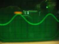
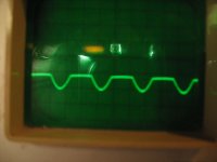
Addendum to Precision Rectifier contd..
Five scope photos are attached. They are numbered 1 through 5 from left to right to second row for identification. These photos track the quality of the positive output pulse signal [for R ch] as a function of the forward bias to its attendant switching diode. This forward bias to the diodes was varied by varying the value of R* from the value of infinite [absent] down to ~12K like that depicted in the previous post. The conditions of this stringent test were:
1. Input sinusoidal signal at 20 KHz.
2. Output pulse voltage Vp = 5 mV for photos 1 through 4. Vp was increased to 10 mVp for photo 5
3. Vertical scale of scope = 5 mV/division. Output signals [1-4] were confined to one graticule of the scope.
Photo 1 shows the ragged pulse output with no forward bias to diodes [ R* absent]. This performance is unacceptable audiologically.
Photo 2 shows the positive output pulse [5 mV] with a 0.25V forward bias to the diodes [R* = 20 K]. Much improved looks over that of photo 1. Still the rising baseline [tilt] to the left is not acceptable.
Photo 3 shows the positive pulse [5 mV] with 0.33 forward bias to the diodes [R* = 15K]. IMHO this is suitable for hi fi audio.
Photo 4 shows the positive output signal [5 mV] with 0.40V forward bias to the diodes [R* = ~12K]. Its look are unlike that in photo 3 [pulses have mostly disappeared], and looks like a sine wave signal. One may conclude that LF356N in conjunction with its diode operated as a linear buffer and not in their intended capacity to enable half wave rectification.
Photo 5 shows the positive output signal [10 mV; and at half the time-scale of photo 4] with a 0.40 V forward bias to the diodes [R* =~12K]. The Op Amp/diode combo is seen to transition to its designated role [of PR] by the flat valleys in the pulses when compared with the pointier-looking peaks.
I listened to music via the current source aP amplifier by using a 0.40V forward bias to the PR diodes; such that the magnitude of the output analog pulses [leaving PR] ranged up to 0.5 Vp each. The system sounded great for me to declare that it is hi-fi to my ears.
The above protocol makes for a stringent test to identify the best Op Amp and/or switching diodes combos; first by using no forward bias voltage to diodes so as to compare the looks of the output pulse signal like shown in photo 1. And then this test allows to fine tune the diodes' forward bias voltage by finding [and using] the correct value for R* in the schematic /circuit of PR [photos 3-5].
I am ready to detail the schematic/circuitry of the stages downrange of the PR; which I hope that I have "exhausted" a lot of detail for it, and done it justice.
Attachments


Back on track at the Inverting Summing Amplifiers
The left image shows the block diagram of the current source aP DC amplifier under discussion. It was reported earlier, and is shown again to get us back on the track of detailing its schematic. We are at the 2 blocks labeled with the Sigma sign. The two blocks mean 2 Op Amp-based inverting summing amplifiers [ISA], which are matched [from a dual unit] and whose input and feedback resistors are inter and intra matched [1 part per thousand in resistance] to sustain accuracy. The middle and right images are two different modes to operate the ISAs, and the circuits downrange of them. Let us look at the middle image first, and focus on the upper ISA for discussion. What applies to it,applies equally to the lower ISA.
1. Upper ISA receives 2 input voltages. A constant DC voltage of -4.6 V from the bias generator. This voltage is inverted and amplified by the ratio of 10K/8.2K to give an output of +5.6 Vdc; clearly destined to drive NPN in downrange circuits. This 5.6 Vdc is forward bias and enables idle operation.
2. Upper ISA also receives a shaded negative pulse signal from Precision Rectifier [PR; output B from past schematic] during its duration spanning 0 to t1 seconds. It is inverted at unity gain [10K/10K] and superimposed on the fixed forward bias voltage [+5.6 Vdc] as depicted in graphic at the output of OA1. Thus one generates an equivalent fixed battery in series with a time-varying battery; such that their EMFs are additive. It follows that the conduction of current in NPNs downrange will always be increased [e.g. at maximum input Vp], and thus will move them in the direction of their saturation.
3. Lower ISA receives an input +4.6 Vdc forward bias voltage, and an additional unshaded positive pulse [output A of PR] in the following or subsequent time duration of t1 to t2 seconds. The graphic at the output of OA2 shows a negative forward bias of -5.6 Vdc onto which is superimposed a time varying negative pulse. This output is destined to drive PNPs in the downrange circuits such that their conduction of current will always be increased; because the depicted series equivalent batteries have additive EMFs like those of the upper OA1 ISA.
Now let us look at the right image for comparison.
1. Same ISAs, and the same application of the fixed forward bias voltage to drive the complementary bjts in the downrange circuits.
2. But; I have reversed the application [polarity] of the pulses from that shown in the schema of the middle image.
3. It follows that the resultant graphics at the outputs of OA1 and OA2 ISAs show pulses which are in series with [aka superimposed on] the desired forward bias voltage ; except that their time varying EMFs oppose or buck that of the fixed forward bias.
4. It follows that the complementary bjts in the downrange circuits will always experience a decrease in current conduction; meaning these bjts will move in the direction of their cutoff..
Both modes of operation have the same building blocks of circuitry, and both have a performance which is fully satisfactory. More on that in the future.
I will proceed with the mode of operation attendant to the Right image to detail the power amplifier which is operated by diminishing and/or decreasing its idle current. I can also demonstrate the amp corresponding to that of the middle image if needed.
Next up are the schema of the current drivers to the output stage per the block diagram.
Attachments

A photo to go along with the previous post
The photo shows a partial frontal view of the amp. Please zoom at the perforated board located at top center. Note the two vertically-aligned pairs of female RCAs which are the pulse signal inputs to ISAs. Each vertical pair [e.g. for the right ch] mates with the pair of male-ended RCA cables emanating from the right channel of the remotely-located Precision Rectifier [PR; see pic of solderless proto board]. Note that I can plug the incoming 2 pulse signals two ways, and thus get the option of the two distinct modes of operation; increased or decreased conduction of current in the downrange circuits like described in the previous post. Come to think of it, I can operate this amp four different ways, increased, or decreased, or via the two mixed; aka increased-decreased conduction of current. The latter means [for example] operating the R ch via increased conduction and simultaneously operating the Left channel via decreased conduction of current. Flexibility of decadence!
Please zoom to the far right of the photo, and locate/note the dual Op Amp [LF353N] which is the 2 ISAs.
Attachments
Driver to the output stage
The left image shows the block diagram of the current source aP DC amplifier under discussion. We are at the next to last block labeled Driver for Output Stage. The right image shows its detailed schematic. Note the following:
1. The schematic of the Inverting Summing Amplifiers [ISA] was simplified.
2. There is an imaginary horizontal line which divides the top from the bottom parts of the schematic so as to signify, and/or invoke symmetry; needed to preserve the accuracy of the pulses.
3. The combination of the forward bias and pulse voltages emanating from ISAs are presented to the compounded bjts [Q1, Q2, Q4 and Q5;they are TO3P] which operate as discrete buffers to ISAs. They also have enough oomph to drive the downrange complementary bjts Q3 and Q6.
4. The color photo shows two pairs of these dual complementary buffers on their perforated board; catering to the Left and Right music channels. It shows that Q1 and Q4 are physically conjoined [back to back], Q2 and Q5 are also conjoined [back to back] with a bolt + spacer passing through their [4] mounting holes.
5. The voltage outputs of this pair of complementary buffers drive the complementary bjts Q3 and Q6 which are affixed to the tunnel heat sink of the output stage.
6. Forward bias and pulse voltages to the inputs of the downrange power output stage emanate from the emitters of Q3 and Q6 as depicted by the graphics; which I'll backup with scope photos.
7. Note that the EMF of each pulse [set at 2Vp absolute] opposes the attendant forward bias voltage that it sits on.
8. As Q6 processes its pulse heading towards zero Vdc at Vp = +2 V, its parent conduction of current at idle decreases to a minimum. Ditto for Q3 when it processes its pulse later on which also heads toward zero Vdc at Vp = -2Vdc.
9. The current flowing through the load resistor [50 Ohm] which joins the emitters of Q3 and Q6 dips to no lower than ~100 mA [by calculation] at either excursion of Vp of the sequential pulses. Thus Q3 and Q6 do not cutoff which is a must. Ditto for the bjts in the preceding discrete buffers.
More detail, scope photos coming up..
Best regards
Attachments

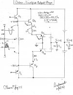
The left image shows the schematic of the driver stage of the previous post [Q3 and Q6] bonding with a simplified output stage. Noteworthy are the following 3 points:
1. The graphic that is shown to the left of the power resistor [50 Ohm ] inter connecting the emitters of the driver's complementary bjts [Q3 and Q6]. It shows 3 important features. First; a complementary forward bias voltage of [plus and minus 3.7 Vdc] to the following bjts. Second; the time variant [sequential] analog pulse voltages which are superimposed on the forward bias voltages. The peak value of each pulse Vp = 2 V. Third, each analog voltage pulse opposes that of the forward bias one which it sits on.
2. The calculation of "idle status" which is shown to the right of Q7. It has 2 important results. First; an idle current of 1.2 Adc flows in the 2 Ohm power resistor which interconnects the the emitters of Q7 and Q9, and an identical 1.2 Adc flows through the second [lower] power resistor [2 Ohm] interconnecting the emitters of Q8 and Q9. Second; the idle voltage drop of 2.4 Vdc [delta V] across each of the 2 Ohm power resistors. In operation, the analog pulses of peak value Vp = 2V sequentially minimize [delta V] say each down to a new value 0.4 Vdc. Said otherwise, [Q7 and Q9] and [Q8 and Q10] sequentially head towards their cutoff; by choice.
3. The center points of the two dual power supply batteries are the power output ports [Vo CB], and Vo' CE]. Their power loads Zl and Zl' splice the sequential analog pulses so as to reconstitute an amplified replica of the parent sinewave signal which was presented to the input signal of the Precision Rectifier.
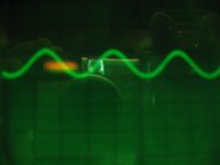
The following scope photos show the objective operation and/or the performance of the output stage. The signals are 20 KHz.
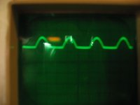
a. The left photo shows the performance at the emitter leg of Q7. The vertical scale is 1 V/div. The flat tops of the pulses reside at the emitter's idle bias value of ~+ 2.4 Vdc. The analog pulses [Vp = 2 V] which are superimposed on this bias voltage head down towards 0 Vdc baseline of the scope; aka to cut off Q7 and series connected Q9.
b. The next photo shows the performance at the emitter leg of Q8. The flat bottoms reside at ~-2.4 Vdc. The analog pulses [Vp = 2V] head upwards towards 0 Vdc baseline of the scope; aka to cut off Q8 and Q10.
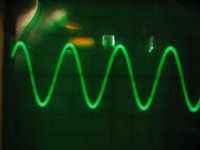
c. The top right scope photo shows the reconstituted sine wave signal [20 KHz] at the power output port Vo-CB; across a non-inductive power resistor [8 Ohm/20 W]. This output voltage [5 V/div scale] is ~16 Vp-p which is commensurate with calculations; meaning this load receives a plus and a minus 1 Amp via the calculation: Vp = 2 V divided by 2 Ohm.
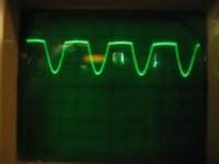
d. The bottom scope photo shows a clipped 20 KHz signal at the same output port Vo-CB across Zl = 8 Ohm. Note its round and/or flat peaks and valleys. I enabled this performance by increasing the analog pulse voltages Vp to a value greater than 2 V; meaning I deliberately pushed the output stage bjts into cut off.
to be continued..
1. The graphic that is shown to the left of the power resistor [50 Ohm ] inter connecting the emitters of the driver's complementary bjts [Q3 and Q6]. It shows 3 important features. First; a complementary forward bias voltage of [plus and minus 3.7 Vdc] to the following bjts. Second; the time variant [sequential] analog pulse voltages which are superimposed on the forward bias voltages. The peak value of each pulse Vp = 2 V. Third, each analog voltage pulse opposes that of the forward bias one which it sits on.
2. The calculation of "idle status" which is shown to the right of Q7. It has 2 important results. First; an idle current of 1.2 Adc flows in the 2 Ohm power resistor which interconnects the the emitters of Q7 and Q9, and an identical 1.2 Adc flows through the second [lower] power resistor [2 Ohm] interconnecting the emitters of Q8 and Q9. Second; the idle voltage drop of 2.4 Vdc [delta V] across each of the 2 Ohm power resistors. In operation, the analog pulses of peak value Vp = 2V sequentially minimize [delta V] say each down to a new value 0.4 Vdc. Said otherwise, [Q7 and Q9] and [Q8 and Q10] sequentially head towards their cutoff; by choice.
3. The center points of the two dual power supply batteries are the power output ports [Vo CB], and Vo' CE]. Their power loads Zl and Zl' splice the sequential analog pulses so as to reconstitute an amplified replica of the parent sinewave signal which was presented to the input signal of the Precision Rectifier.
The following scope photos show the objective operation and/or the performance of the output stage. The signals are 20 KHz.
a. The left photo shows the performance at the emitter leg of Q7. The vertical scale is 1 V/div. The flat tops of the pulses reside at the emitter's idle bias value of ~+ 2.4 Vdc. The analog pulses [Vp = 2 V] which are superimposed on this bias voltage head down towards 0 Vdc baseline of the scope; aka to cut off Q7 and series connected Q9.
b. The next photo shows the performance at the emitter leg of Q8. The flat bottoms reside at ~-2.4 Vdc. The analog pulses [Vp = 2V] head upwards towards 0 Vdc baseline of the scope; aka to cut off Q8 and Q10.
c. The top right scope photo shows the reconstituted sine wave signal [20 KHz] at the power output port Vo-CB; across a non-inductive power resistor [8 Ohm/20 W]. This output voltage [5 V/div scale] is ~16 Vp-p which is commensurate with calculations; meaning this load receives a plus and a minus 1 Amp via the calculation: Vp = 2 V divided by 2 Ohm.
d. The bottom scope photo shows a clipped 20 KHz signal at the same output port Vo-CB across Zl = 8 Ohm. Note its round and/or flat peaks and valleys. I enabled this performance by increasing the analog pulse voltages Vp to a value greater than 2 V; meaning I deliberately pushed the output stage bjts into cut off.
to be continued..
Attachments

Still at it for the broadest view of performance
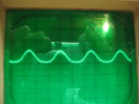
The left image shows the simplified schematic of the driver-output stage. It differs from the schematic I showed in the previous post by the "graphic which is shown to the left of the 50 Ohm power resistor that is interconnecting the emitters of Q3 and Q6. The voltage of the sequential analog pulses is superimposed on the forward bias voltage to bjts and adds or augments it so as to increase the conduction of currents in the driver and the output stage bjts. The peak voltage value of the analog pulses was chosen to be Vp = 2V.
Thus the following scope photos show:
a. The left photo shows the performance/operation at the emitter leg of Q7. The frequency is 20 KHz, and the vertical scale is 2V/div. The flat baseline of the pulse is the idle bias voltage of Q7 at ~3 Vdc which is delta V [ 2.4 V across 2 Ohms] plus one Vbe [0.6 V that of Q9] above ground; which is also the zero voltage baseline of the scope. The positive pulses rise upward to a peak of ~5.7 Vp of delta V plus one Vbe. This means 1 Amp idle plus another 1 A peak across the 2 Ohm power resistor.
b. The right photo shows performance at the emitter leg of Q8. The flat baseline is the idle bias of Q8 at~-3 V which is delta V plus one Vbe below ground or below the zero baseline of the scope. The negative pulses dive to more negative value at -5.7 Vp which corresponds to delta V plus one Vbe. This means 1 Amp idle plus 1 Amp peak across its 2 Ohm resistor.
c. The middle photo is the power output voltage at Vo-CB across the 8 Ohm load resistor. It is ~16 Vp-p [20 KHz] on the 5 V/div vertical scale. Again, the load resistor splices the analog pulses so as to recreate an amplified replica of the sinewave signal which was input to the Precision Rectifier.
* At idle the measured voltage of either dual PSU is ~44 Vdc. It droops by ~2-3 Vdc with a 20 KHz because of "increased" conduction of current in the output stage. By contrast to the other mode of operation of the previous post, the voltage across the PSU rises by ~2-3 Vdc due to decreased conduction of current in the output stage. Makes perfect sense, and has implications!.
Now I am ready to finish detailing the output stage of this current source aP DC amplifier.
Attachments


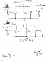
Detail of Output Stage
The image details the schematic of the output stage of the current source aP DC amplifier, with more focus on the two power supplies which cater to it. All of the bjts are TO-3 [except Q3 and Q6 = TO-3P] sit on the tunnel heat sink described earlier. I spoke early on of a Left and Right branches. For the example of the Left branch one sees Q3 driving the 2 NPNs [2SD287A], which then connect via their 2 emitter resistors [4 Ohms, 50/W] to PNPs [MJ15027] operating in common base configuration. The Right branch bjts are complementary left to right; but not top to bottom; which could have been in an ideal world.
The lower and upper dual power supplies provide [each] a maximum of plus and minus 25 V; a voltage limit imposed by the rating of the filter caps of 0.1F/25V of the lower PSU. The toroid power transformer of the lower PSU would have given +/- 50 Vdc, and thus the deliberate use of a variac [setpoint of 50 - 60 Vac]which energizes its primary winding, and also the other 3 primary windings of the 3 power transformers of the remaining 3 dual PSUs. The power output ports [Vo and Vo'] are the center connections of their series connected filter capacitors which connect to the Center Tap of the secondary winding of the power transformer. In practice, I have a 2A fast-acting fuse at each port so as to protect the loudspeaker loads.
One may ask why does the upper power supply have capacitors of lower storage values [0.015 F] compared with the capacitors of the lower PSU [0.1F]. The focus of the early hobby work was to operate the upper set of bjts in common collector configuration, and to derive the spliced output signal from the lower set of bjts operating in common base configuration. In my mind, the "quality" of the lower PSU mattered more that the upper one!. Ditto for the CB bjts as compared with the CC bjts.
I am glad that I shared with y'all an accurate, and [hopefully] a clear blueprint of this current source aP DC amplifier. There will be additional analog pulse amplifiers.
Coming up will be the equally important subjective performance. How's it sound?
Attachments
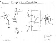
Summary, connections and talk of distortion
I showed the left image in an earlier post. It does a great job at summarizing the structure and operation of the " current source AP amplifier" [CSaP amp] under discussion as follows:
1. A sinusoidal signal is input to a dual half wave Precision Rectifier [PR] which slices it cleanly relative to common into an independent positive and negative going analog pulses or signals.
2. The negative-going pulse is first presented to a forward biased PNP during its allocated time interval of 0 to t1 seconds.
3. The positive-going pulse is presented next to a forward biased NPN during its allocated later time interval of t1 to t2 seconds.
4. The complementary bjts of the above power output stage operate in a common emitter opposed collector configuration.
5. The load [R] at the power output joint of the opposed bjt collectors, splices the analog pulses so as to reconstitute an amplified replica of the sinusoidal signal which was input to PR.
I then substituted [on paper] N, and P channel MOSFETs for NPN and PNP respectively. I also simplified the resultant schematic which is shown in the top part of the right image. I have two objectives attendant to this right image:
1. Relate its structure-operation to that of the Pass Zen Amplifier which happens to be 20 years young. The bottom part of the right image shows my oversimplified schematic of the Pass Zen amp in which I also used a dual PSU [instead of one in the classic parent] to ease the subjective comparison with CSaP amp above it. Both simplified schematics of the output stage are structurally similar.
2. Address sources of distortion in CSaP amp.
Here I go:
1. The N device in CSaP operates much like that N in Zen because both are processing a positive going pulse [shaded] during the allocated time interval of 0 to t1 second. Simultaneously, the P devices in both schema operate equally alike as constant current loads to each of the N devices.
2. As the polarity of the input signal goes negative to the N device in Zen, it continues to be processed by this N device with its P device still operating as a constant current load.
3. By contrast, the N device in CSaP is denied processing the negative going pulse in the time interval of t1 to t2 seconds in favor of presenting it to the gate of the P device in its circuit.
4. Now the P device in CSaP amplifies this negative going pulse while the N- device plays the new role of a constant current load to the P device in this circuit.
5. The operating roles of N and P devices in CSap flip-flop or interchange predictably as a function of the polarity of the analog pulses. By constrast N and P devices in Zen stay steadfast in their preset roles.
I found no evidence of cross-over distortion in this type of amp. But, I can see that distortion in this power output signal can easily happen if; for example the transconductance of the N and P devices are different. The effect of this variable can be described informally as a different ratio in the size of the shaded to unshaded pulses in the reconstituted sinusoidal signal. Meaning the shaded portion of the power output signal is smaller or larger [electrically] that the unshaded negative pulse; which were equally sized in the parent input signal.
to be continued..
Attachments
- Home
- Amplifiers
- Pass Labs
- Class aP amplification