just to let you know that you aren't alone in this thread
even if matter is out of my actual interests ,and slightly above my head

even if matter is out of my actual interests ,and slightly above my head
Hello Zen Mod. Thank you for your feedback and continued reading of my posts. I've debated in the past which Forum to include this style amp. Will it best to have it in Pass Labs or Solid State or Vacuum Tubes? It has information which belong to each one. I chose Pass Labs because I got to know the crowd from the diyF6 thread. Competition for readership? You bring forth a good point for any DIYer to reflect on "interest" in any topic or not.just to let you know that you aren't alone in this thread
even if matter is out of my actual interests ,and slightly above my head
I am looking forward to assembling a Class aP amp with 2SJ28s. I do not have 2SK82s [or vacuum tubes] which will readily replace R085s in the amp of the past post. This solid state amp with 2SJ28 will attempt to mimic a Class B triode amp; nothing fancy or fancier
Best regards.
N.B. There's interest among DIYers in the sound of triodes via solid state amplification. They crave this sound per their high interest [and it shows] in the Pass Class A amplifiers. I am reacting to their "interest" by further broadening the scope of application.
Last edited:
even if I'm not so active ( read- annoying  ) in other foras/forums/fora/foorahs/whatever , I believe there is best place for whatever you want to write about
maybe least amount of mine is bigger approach here** .......
**well , maybe burst or two, here and there ........
) in other foras/forums/fora/foorahs/whatever , I believe there is best place for whatever you want to write aboutmaybe least amount of mine is bigger approach here** .......
**well , maybe burst or two, here and there ........
Last edited:
even if I'm not so active ( read- annoying
maybe least amount of mine is bigger approach here** .......
**well , maybe burst or two, here and there ........
Thanks Zen Mod for the advice; namely post in a Forum where the content fits best. Will do.
I am glad to stay this/same course.what I meant - keep it here
One more Class aP amp to assemble.
The amp of the previous posts is well characterized. Thus, its last posted schematic is final, and is an actual working blueprint of a Class aP amp which works beautifully and reliably. It paved the way for this upcoming amp which is described as follows:
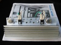
1. The two left photos show the power output semiconductors 2SJ28 and IRFP9140 [P-Mosfet] on a generous heat sink.
2. There is room on this heat sink to install TO-220 or other PNP [not TO-3] to be used later instead of IRFP9140 so as to broaden the scope of application.
3. The far right image is a simplified schematic of the power output stage, and shows the the Op Amp drivers and the power output transformer.
3. Had I used 2SK82 in the amp of the past posts instead of R085, this one in this post would be characterized as its functional complement.
The next post will report its working prototype.
The amp of the previous posts is well characterized. Thus, its last posted schematic is final, and is an actual working blueprint of a Class aP amp which works beautifully and reliably. It paved the way for this upcoming amp which is described as follows:
1. The two left photos show the power output semiconductors 2SJ28 and IRFP9140 [P-Mosfet] on a generous heat sink.
2. There is room on this heat sink to install TO-220 or other PNP [not TO-3] to be used later instead of IRFP9140 so as to broaden the scope of application.
3. The far right image is a simplified schematic of the power output stage, and shows the the Op Amp drivers and the power output transformer.
3. Had I used 2SK82 in the amp of the past posts instead of R085, this one in this post would be characterized as its functional complement.
The next post will report its working prototype.
Attachments
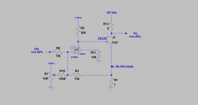
The attached circuit was used to determine the electrical properties of 2SJ28s, and to find pairs [hopefully] with similar performance. Please note:
1. U1 and U2 are the 2 Op Amps in OPA2134
2. The idle current of OPA2134 is ~8 mA entering its +Vc terminal and exiting its -Vc terminal. Both Op Amps share this idle current.
3. A load resistor [300 Ohms] is inserted between +15 Vdc [regulated] and the chip's +Vc port. The idle current of the chip generates a voltage drop across this load resistor.
4. The new +Vc presented to the chip measures 12.82 Vdc and is the same as Vgs for 2SJ28.
5. This new Vgs or +Vc can be changed up or down relative to ground with a current injected to the summing junction of the left [or right] Op Amp via the 270 K resistor connected to the 10 K pot on far left of schematic.
6. A +15 Vdc connection to the top of the 10K pot decreases the idle current of OPA2134 and thus increases +Vc or Vgs which moves the SIT towards a decreased current conduction.
7. A -15 Vdc connection to the top of the 10 K pot increases the idle current of OPA2134 and thus decreases +Vc or Vgs which effects an increase in current conduction of the SIT.
8. A positive going analog pulse is presented to the non-inverting ports of both Op Amps. Their power output NPNs work in the common emitter configuration. The resultant analog pulses which appear at [their collectors] are negative going with a gain of 3.
Here is a method used to characterize 2SJ28:
1. Turn power to Op Amps.
2. A constant Vgs equal to 12.82 Vdc is present at the gate of SIT. It protects it.
3. Turn power to SIT using a variac-controlled -Vee power supply starting at ~-25 Vdc. The source of -Vee is the power supply of the aforementioned Radio Shack receiver.
4. Monitor the voltage drop across the 1 Ohm load resistor at the drain of 2SJ28. It gives Idss.
5. Increase -Vee in small values and monitor Idss until the onset of SIT conduction [~0.1 mA]. Note the value of -Vee
6. Increase Idss to the values of 25, 50, 75 and 100 mA and record the attendant -Vee which effects each idle current.
7. The data of points 2, 5, and 6 are characteristic properties of the DUT 2SJ28.
8. While at each idle current level of 2SJ28 [as in point 6], apply 100 Hz analog pulses [from Precision Rectifier] to the non-inverting ports of Op Amps so as as to give a -1 volt peak [use scope] at the the gate of 2SJ28. This negative going analog pulse signal is superimposed on the fixed bias of 12.82 Vgs of SIT.
9. The new peak value of Vgs of 11.82 V [or +Vc for OPA2134} generates a peak load current across the 1 ohm drain load resistor. On the scope it is the same as peak drain current.
10. Transconductance is the peak current in Amps per the -1 Volt change in Vgs.
11. Transconductance varied with peak drain current and with -Vee = Vds. I calculated ~0.4 A/V for a unit on the heat sink shown in the previous post. The profile of transconductance thus generated at the different idle currents of SIT are one more characteristic property of it.
I have 6 2SJ28 units and will characterize'm before I assemble the amp. Unfortunately, both 2SJ28 on the heatsink shown in the previous post are, or appeared to be highly mismatched per this method.
Attachments

Last edited:
Power Amp Using 2SJ28 SITs
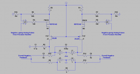
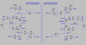
The first step converted the Precision Rectifier [PR] which generated positive-going analog pulses [from an input sine or square etc..signals] to one which generates instead negative-going analog pulses. It was readily done as follows:
1. The schematic to the left of the vertical center divider is a PR which generates positive-going pulses. I've used it in all of the experiments leading to this post.
2. The right schematic is the new PR which generates negative-going pulses. It has the identical components as the left schematic. The only difference is WIRE A which emanates from the upper steering diode [gives +Vp] of left schematic now terminates at the inverting input of the Op Amp buffer of right schematic [becomes -Vp]. Similarly, Wire B which emanates from the lower steering diode [gives -Vp] of left schematic drives the non-inverting Op Amp buffer of the right schematic [stays -Vp].
3. Note that I have attached to each analog pulse output [Vp] a notation for a time interval; e.g. -Vp [0 - t] and -Vp [t - t1]. It means the resultant analog pulses are not concurrent; but are sequential instead.
The new PR which generates negative-going analog pulses drives the output stage of the power amp using 2SJ28 SITs. This will be shown in the next post.
Attachments
Power Amp Using 2SJ28 SITs
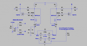
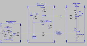
The attached schematic is the output stage of the power amp using 2SJ28 SITs. The SITs cascode the P-Mosfets IRFP9140; or the SITs operate in common gate configuration while simultaneously, the embedded Mosfets therein operate in common source configuration. The objective of this amp is to mimic the operation of a triode vacuum-tube power amp. Note the following:
1. The idle current of each leg [IRFP9140/2SJ28] is 100 mA. It is readily adjusted [up/down] by using the circuit shown at the bottom left of the schematic. Each leg does not cut-off in operation. Both legs imitate power output devices operating in a Class A amp.
2. Local feedback was readily used. It emanates from the junction [source of Mosfet/gate of SIT], to the junction [drain of Mosfe/-source of SIT].
3. The power output transformer is the same used earlier which is made by TRIAD Magnetics.
4. Overall loop feedback is taken from the secondary of the transformer to the inverting input of the front end Op Amp LF356N.
5. The SITs are not matched, and most probably the Mosfets too. At 100 mA idle, Vgs of the SITs is at ~13 Vdc, but one differs from the other by ~1 Vdc.
Now I grasp the hoopla surrounding SITs. The sound of this amp driving a 3-way loudspeaker had a unique subjective performance which I have not heard before. It is noiseless, highly detailed and was louder than the scope measurements [amplitude of Vout] suggested. The amp was stable against oscillation.
I will have objective measurements to report like open and closed loop gain.
Attachments

The voltage gain of the amp was determined as a function of local feedback, and as a function of the value of the feedback resistor [Rf] emanating from the secondary winding of the power output transformer and ending at the inverting input of LF356N Op Amp front end of the precision rectifier.
1. -Vcc was equal to 75 Vdc. No local feedback was used; meaning the gates of 2SJ28s were grounded.
2. Test frequency was 100 Hz, which allowed measurement of circuit voltage with a multimeter.
3. Vi was taken at the inverting input of LF356N [from function generator; sine], and Vo was measured across the secondary winding of the transformer loaded with 4 Ohm power resistor.
4. Voltage gain was Vo/Vi.
5. Open loop gain = 46 at an infinite value of Rf.
6. Closed Loop Gain [CLG] = 17 at Rf = 3.3 K.
7. CLG = 9.6 at Rf =1.5K
8. CLG = 8.4 at Rf=1.3 K [1K+.3K]. This was chosen for music playtime. Open loop gain was reduced by an adequate factor of 5.4.
9. CLG =6.7 at Rf = 1 K. No oscillation at this maximum overall negative feedback.
10. The multimeter did not discern an effect by local feedback. But. this local feedback was discernible when 8 Ohm load resistors were used instead of the transformer. Local feedback was used for music play anyway.
The power rail was raised to -80 Vdc, and music was played. The sound of this system via 3-way ADS730 loudspeaker was highly detailed. Its low end was tight and had a full body[ not anorexic or thin]. The amp was louder than expected; maybe because the SITs are loaded with the transformer; akin to chokes.
Attachments
An ostrich experiment
Do the SITs affect the [subjective] sound of the power amp described in the previous post? I pulled the SITs out of the circuit and then heard the impact of their absence. The attached schematic shows the output stage of the power amp using only IRFP9140. The operating conditions of -Vcc = 80 Vdc, and a feedback resistor of 1.3 K were used like in the case of the power amp containing SITs.
The sound of this [IRFP9140-only] amp is highly detailed, and crystal clear. Its bass is tight and highly articulated. It sounded like a solid state amp. But, this amp sounded different across the audio spectrum from that containing the additional SITs.
Another experiment for me to do will be to use only 2SJ28s in this power output stage.
Attachments
PowerAmpIRFP9140A
The attached schematic is for another functional analog pulse prototype amp. I removed the power output transformer and used instead 8 Ohm load resistors. Note the following:
1. I borrowed a Zen amp approach like that used by Mr. Pass.
2. A full range loudspeaker [FRL] is modeled as a resistor in series with a coil.
3. FRL is two 15 inch musical instruments connected in parallel, and bolted to the ceiling as previously described [4 Ohms net Z].
4. This FRL-power amp combo sounded clear, detailed, and a bit bass shy [because FRLs are bipolar] .
This is a current source power amp. It is stable, noiseless [no hum buzz] and is best suited to drive FRLs. It sounded off-key driving the 3-way boxed L730 loudspeaker.
Attachments
Antoinel interesting stuff but why wouldn't you use the sit as the active gain device instead using it the cascode? Driving the sit in common gate as a cascode is probably not going to allow their benefits to come through.
Hello kasey197, and thank you for your encouraging post. I hope to use only 2SJ28s in a common source configuration by using the attached circuit which I already described in the post of October 12th.Antoinel interesting stuff but why wouldn't you use the sit as the active gain device instead using it the cascode? Driving the sit in common gate as a cascode is probably not going to allow their benefits to come through.
In the short term, I have additional analog pulse power amps using Mosfets to report.
Best regards.
Attachments

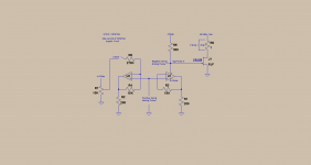
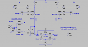
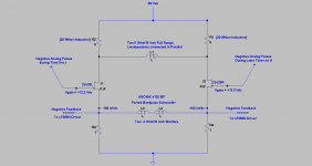
The attached schematic shows one half of the power output stage which will use only 2SJ28 SITs. The second half is exactly its mirror image. Like before, the objective for this prototype is to mimic a power output stage which normally uses triodes by using SITs instead. Please note the following explanation on its works:
1. U1 is Op Amp LF356N.
2. The +V pin of LF356N is connected to +15 Vdc via a 300 Ohm load resistor.
3. The NPN of the power output stage of LF356N is used in the common emitter configuration [has local gain]. The 100 Ohm resistor which connects the output of LF356N to ground goes to the emitter of NPN, and the 300 Ohm resistor connects to its collector. This NPN inverts the phase of Analog Pulses [APs] which are presented at Vin.
4. A positive bias voltage ~13 Vdc develops at the gate of 2SJ28 relative to its source. The idle current of LF356N passing through the 300 Ohm load resistor is partly responsible for this bias, and is tweaked [down to a lower value for example] by increasing the conduction of NPN [in LF356N] with the 10 K/150K adjuster that is shown at the bottom left of the schematic.
5. LF356N is used as/like a classical inverting Op Amp. Its inverting port is grounded, and it non-inverting input is instead the summing junction. This summing junction nulls equal in amplitude and opposite in phase APs to match the zero volts at the inverting input. This summing junction at the non-inverting input of LF356N also nulls the +ve voltage presented to it by the bias adjuster with the resultant negative voltage at the source terminal of 2SJ28.
6. The resultant adjustable negative voltage of 50-100 mVdc at the source of 2SJ28 gives this SIT its fixed idle bias of 50-100 mA.
7. And so, the resultant negative-going APs at the source of 2SJ28 ride in one direction atop this fixed voltage bias; meaning the SIT does not turn off.
In the event point 5 is ambiguous, use up and down arrows to follow the AP signals so as to make sense why the Op Amp is used as shown. This building block is stable against oscillation. I'll assemble its mirror image, and move on to test the resultant power amp; initially with 8 Ohm load resistors, and later with a power output transformer.
Attachments
A prototype power amp using only 2SJ28s power output devices was assembled on a solderless protoboard. It is fully functional, and sounds great. But first, please note the following in the attached schematic.
1. The schematic is one half the power amp. It amplifies analog pulses in the time duration of 0 to t. The other half is identical to it, and amplifies analog signals in the signal time duration of t to t1.
2. The input Vi are Positive Analog Pulses [APs].
3. I show the 1/2 amp as 3 distinct interconnected circuits.
4. The bottom left is the circuit to adjust the idle current of 2SJ28L. It also increases the conduction of NPN power output in LF356N; augmenting its Class A operation.
5. The middle section is the voltage driver of the power output. The intrinsic idle current of LF356N was ~4.5 mA. It was increased by the bias adjuster to ~11 mA. The resultant voltage drop across the 300 Ohm load resistor is ~Vgs of 2SJ28L.
6. The right side of the schematic is the power output stage. All tests were done with a - 50 VDC power rail.
7. Both sections of the power amp were tested individually. Note the idle conditions in fine print for DC voltages. The overall, and the in-process voltage gains were identical [force-matched]; because of negative feedback.
8. A Gate voltage of ~12.2 Vdc enabled [via adjuster] an idle current of 100 mA in 2SJ28L; where L denotes left in the final combined schematic.
9. 2SJ28R also idled at 100 mA by using its independent bias adjuster. Except its Gate voltage was ~13.3 Vdc by comparison with 2SJ28L.
The complete power amp was stable against oscillation, and so were its quiescent conditions; e.g. the idle bias of each section at a rock solid 100 mA. I'll show photos of the amp, and its applications which I hope will be interesting.
Attachments
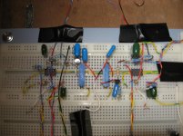
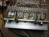
The photos of the prototype amp using only 2SJ28s in the power output stage are attached. Not pretty, but this prototype like others before it is readily modified [to optimize], and is fully operational as shown.
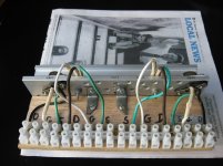
1. The left photo shows the 2 drivers of the two 2SJ28s. A vertical line drawn between the two 10K trimpots in the center of view separates the independent drivers. Each driver has its own LF356N, and its idle current adjuster or its 2SJ28.
2. The right photo shows the 2SJ28 TO-3 devices on the heatsink. The Mosfets of past practices [IRFP9140] sit on the same heatsink, and are not involved.
Let's talk about the pleasing sound of this prototype in the next post.
Attachments
PowerAmp2SJ28BB
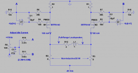
The schematic of the power output stage using 2SJ28s, and its loudspeaker loads is attached. I have omitted the circuitry supporting it for clarity. Please note.
1. Each 2SJ28 idles at 100 mA c/o its independent bias adjuster.
2. The gate voltage for the left and right 2SJ28s was/is +12.2, and +13.3 Vdc respectively.
3. Negative-going analog pulses [APs] are simultaneously superimposed on the gate voltages of the 2SJ28s. This direction of signal moving towards ground increases the conduction of 2S2J28s. Still, both 2SJ28s go back to idling at 100 mA each in operation [as seen on scope at their sources], and thus do not cut off.
4. A full range pair of drivers interconnects the two drains as shown. They are unenclosed, and thus are dipolar in their operation; meaning their bass output is weak by cancellation of their front and back waves.
5. A commercial band pass ported subwoofer interconnects the sources of the 2SJ28s. Sits in the corner of the room.
6. The indicated phase dots on the voice coils [modeled by inductors] gave an augmentation of bass output, and thus generated a balanced overall sound; which was clear and detailed.
I am toying with light bulbs to replace the 8 Ohm/20W non-inductive loads at the drains of the 2SJ28s. This is nothing new and is a well established teaching by Mr. Pass, Mr. Rothacher, and DIYer wrenchone in their DIY amps. I'll keep you posted.
Attachments
- Home
- Amplifiers
- Pass Labs
- Class aP amplification