I agree. Yes. That's true.
Only all the voltages that are recommended to be set - R1, R9, R7 ... are actually set currents - Ohm's law and it's all DC.
During the first setting, it is not necessary to monitor the alternating component and it is not necessary to connect the signal generator.
When the recommended voltages and currents are well set, you can play with the generator and explore other options.
@Fero_11
Thanks for the tutorial. I think I indeed didn't go through part I of the original paper again enough times.
DRV+ & DRV-, I see which also mean the voltage across Z3 & Z4 respectively, I got a perfectly aligned 0.25V at both zener diodes at one channel.
The other channel was also perfectly aligned at around 0.25V, but after I restart to test again with IN+ also grounded, it went to back to its old problem: I could not really align + and -, R7 R8 measured voltage would generally have 0.2V difference and DRV+ DRV- at 0.125V and 0.25V. But I guess this is not really critical.
For this channel if I want to go really low on output offset voltage, R7 R8 basically need to go at least 1.4V. The other channel seems to pull and balance itself symmetrically.
I am going to test the rest with one pair of output stage on when the chassis parts are sent back.

Thank you guys for helping out. That helped my getting to know oscilloscope easier.
I think I should be able to see it up and running for this end of year holiday season.
I think I should be able to see it up and running for this end of year holiday season.
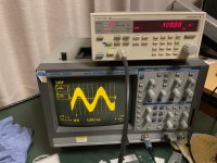
50 Hz, line frequency?@BDP
Here is the wave form at DRV.
I got this same wave form for DRV+ DRV- and OUT at both channels.
IN+ and IN- both connected to GND, no signal input.
Curiosity got the better of me. Plus, it's been a long time since I built the amp and had it apart for cleaning..
So, I took the cover off. Removed the fuses to the output stage. Removed the R81 output stage feedback jumper. The output stage was wired but not powered.
Switch in unbalanced mode. Shorted the (+) inputs.
Checked the DC voltages across the biasing resistors.
R9 and R10, 10 mA feeding each differential pair, check, the same as 20 + years ago. Wow
R7=1.063 volts, R8=1.066 volts. divided by 47.5 ohms, about 22mA bias. Check
Output offset 20mV measured between R23 and R24. Check
DC drive voltages. +DRV, 4.00v. -DRV, 4.05v, Check
Connected signal generator to + input of one channel at 25mV, 1Khz. Output measured between R23 and R24 equaled 0.727vrms.
For a gain of 29.08. check
Distortion was .02% The front end is operating folded cascode with R21, R22 at 100 ohms
Looking with the scope set to DC mode I see the wave form at the drive terminals shifted the +/-4 volts dc. Between R23 and R24 (output of front end) wave form with no dc. Well, 20mV
First pic is 5 volts/div. One scope channel at +DRV and the other channel -DRV.
Second is 0.5 volts/div of the output between R23 and R24. You can see its half the DRV level.
NOTE: When R81 was in (shorted, max feedback) there was some interaction between the non-powered output stage and the frontend, and it appeared that there was no signal present to the feedback network?? I measured a gain of 45 at the DRV terminals.
Attachments
Earlier with output stage not connected I got 4.xV at one side of DRV and 2.xV at the other end. (measuring each DRV against GND)
The figures for the 2 channels varied a bit but anyway they are far from equal.
We'll see when I connect the output stage.
The figures for the 2 channels varied a bit but anyway they are far from equal.
We'll see when I connect the output stage.
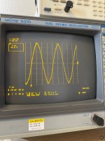
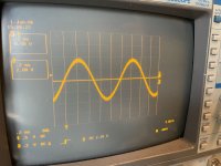
Hey everyone, I wired up with one pair of output stage and tested.
With signal input connected (signal generator), I got a Sine that looked pretty Sine and time interval is correct, 1kHz, although it looked a bit noisy, probably because I forgot to check again output offset when I tuned the trimpots a bit?
Belows are what I measured this time.
R8 ~0.9V R7 ~1.1V
No R81
Sine wave input 100mV
+DRV 0.69V -DRV0.55V
R34 R35 0.018V
But I still only get noise when I tune signal level down to some 30mV. At least things seem to be working.
Next I am sending those long bars to drill open some holes so they become proper bus bars, and buy one more DMM, it will make precisely tuning R7 R8 more doable, then I will wire up the whole thing for the final setup. Maybe it can be up and running this end of year vacation.
Just want to share.
Attachments
A75 is an ambitious project. If that's the output we're seeing on the scope that looks like oscillation. If that's the case, C9 and C10 may be needed to add some lag compensation to stabilize it. Refer to the article about values to try and also the comment about the gate resistors on the MOSFETs.
When you measure +DRV and -DRV, the important thing here is the level of potential (voltage) between them. We're not referencing to ground there. You will want to place one DMM probe on +DRV, and the other DMM probe on -DRV. What is this level of DC voltage? The article says.... "Verify that the DC voltage across + DRV and - DRV is about 7V. If it is greater than 8V, you may have a problem...." Remember that the conduction requirement is that voltage Gate-to-Source will be about 3.5-5V in a MOSFET. This conduction will happen quick so we always start low and "sneak up" on the final setting or else the output stage can easily draw way too much current and bad things will happen.
When you measure +DRV and -DRV, the important thing here is the level of potential (voltage) between them. We're not referencing to ground there. You will want to place one DMM probe on +DRV, and the other DMM probe on -DRV. What is this level of DC voltage? The article says.... "Verify that the DC voltage across + DRV and - DRV is about 7V. If it is greater than 8V, you may have a problem...." Remember that the conduction requirement is that voltage Gate-to-Source will be about 3.5-5V in a MOSFET. This conduction will happen quick so we always start low and "sneak up" on the final setting or else the output stage can easily draw way too much current and bad things will happen.
So I got my additional DMM. It really is the correct way to go.
The channel I was testing always has a 23~26mV gap when output stage disconnected. I think not an issue.
Voltage across Z3 and Z4 (DRV) was some 5.9V.
With 1 pair of output stage connected this time I got a clean signal. Input was same 100mV Sine wave.
The voltage I got at output resistor R34 was some 0.010V, voltage across DRV also was some much less than 1.0V number.
But R7 R8 seemed to have dropped to ~0.5V so I guessed it just needed some tuning after output stage was connected.
I stopped here for a funny reason: I didn't have no more test lead clips to tune R7 R8. I used all my clips to hook up the cables at output stage.
Now I will just wait until those bus bars are sent back from the machining shop.
I got an interesting audible oscillation at the transformer when output stage was not connected. It was a steadily periodic high pitch to low pitch sudden dive, a complete cycle was roughly 6 seconds. It disappeared after output stage was connected.
Attachments

I got a question here: what resistance value of volume knob do you use?
I am studying to try figure this out mathematically at the moment.
Though it looks like 50k, 10k are pretty safe value for transistor amp, I am taking this carefully. The attenuator I am looking to buy is made to order with some lead time, and a little bit expensive.
I am studying to try figure this out mathematically at the moment.
Though it looks like 50k, 10k are pretty safe value for transistor amp, I am taking this carefully. The attenuator I am looking to buy is made to order with some lead time, and a little bit expensive.
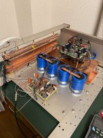
Some updates and a question about output offset voltage.
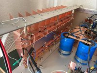
My output stage design turned out to be a pretty stupid design, took lots of effort putting it together and making sure nothing is shorted.
But it worked. Still got one channel to go.
So I got this confusion with output offset voltage.
I have the whole output stage connected and P3 set to maximum, readjusted R7 and R8 from scratch again to ~0.93V and managed to get low output offset in both 100mV and 30mV 1KHz Sine wave condition. Don't recall exact number but definitely < 50mV as suggested in original text. +DRV -DRV was some ~6.01V.
But do we still measure output offset voltage after P3 is set? (~170mV for R34)
Probably not since as P3 opens R34 starts conducting more current and it returns to ground so it won't be near zero?
I measured ~0.8V DC with 300mV Sine wave input and ~0.6V with signal generator & oscilloscope physically disconnected to the amp.
Attachments
Hi Seann,
I appreciate your enthusiasm for this project. It's not the easiest amplifier to build. But the sound is worth the effort. The original documentation describes the setup quite well. Of course, it takes patience and time to set up this amplifier correctly. I designed the PCB myself and I also have differently numbered components in the schematic. But the setup was relatively easy and quick.
My advice:
1. Short the input to GND
2. Check the PWR +REG and PWR -REG power supplies to see if they are OK and symmetrical. For now, it doesn't matter if you have +-40V, +-50V or higher voltage there. The symmetry and filtering are more important.
3. Adjust the P3 trimmer so that the transistor Q11 is almost fully open - this will reduce the bias on the output transistors. On resistors R34 and R35, the voltage is about 50mV or less - you won't be able to fire the output transistors if you have a mistake somewhere. Don't measure it against GND, but directly on these resistors.
4. Then you need to find the best setting with trimmers P1 and P2. I used 10-turn precision trimmers. You really need to play around with it. Turn one first, then the other. Until you get crazy. Or until it's perfect. Set the voltage on resistors R7 and R8 to about 1V with them and also the DC offset on the output as low as possible. For me, it was below +-10mV. Still without a generator connected and with a shorted input.
5. Again, I recommend checking the wiring carefully. There have been hundreds of these amplifiers built all over the world and probably with successful results.
Attachments
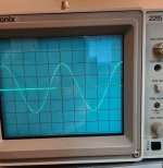
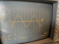
I got our good friend multi-turn trimpot Bourns 3296, and tried tuning R7 R8 using DMM and oscilloscope these few days. Here is what I found and learned (and still learning).
My Sine wave remain clean thin line up to R7 R8 roughly ~0.50V, further going up the Sine wave will go noisy. I tried turning the trimpots in different directions and proportions, the waveform noise seems inevitable.
Aside from noisy waveform and some ~2V DC offset, there seems to be no other problem.
At some point it occurred to me the first time I got the Sine wave on oscilloscope.
I was able to get a clean wave at R7 R8 ~0.9V back in #93 in this thread, and with 25 mV DC offset. At that time I had only one pair of output stage connected. Assuming nothing broke along the way til today, my A75 condition has not changed. I also assume I set the oscilloscope correct at that time and that 25mV DC is credible.
So now it got me interested and one way I might find out is disconnect output stage pairs 2 pairs at a time and see, is it there is some integrity issue with my poorly assembled output stage, or somehow my long circuit (all those cabling on the MOSFET) caused this problem that once output stage pairs build up, something go wrong?
Or, I can do that while assembling the remaining channel, measuring with each pair installed.
I have disconnected 4 pairs of output stage so far, what I got on the oscilloscope is still the same. So my suspicion with assembly integrity is getting weaker. And with P3 going maximum I still got same noisy waveform once R7 R8 past ~0.53V. Some how now when that front stage current feed go past 10mA the waveform starts getting noisy.
Attachments
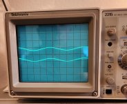
@Fero_11
Thank you as always.
What I found interesting was that DMM seem to become a significant load to my circuit.
My reading on R7 and R8 will bounce when I only connect to one of them, because the value always drift when I connect the other side with DMM, and then settle. Maybe with both sides loaded they are now settled?
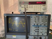
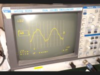
So here came the question, that how many DMM is enough? Because I still need to measure DC offset. This was also the point I started thinking hmm that mighty oscilloscope should be able to measure offset voltage right? I had tried no input signal and input grounded, now I could try tuning it using the scope.
Anyway I still tried, by tuning R7 and R8, then disconnect and check DC offset.
I was able to find a point of low DC offset, though that offset generally drifts a lot, even after letting it settle. And this attached image is what it looked like. Unfortunately I didn't wait longer see if the waveform could settle.
But I think I didn't set the scope to 10x, which is the probe I am using, so that DC should be multiplied by 10, which is still 0.96V, quite a lot.
And I was looking for consolation that DC offset is just an offset it will not end the whole system ha ha: https://www.diyaudio.com/community/threads/amplifier-dc-offset-how-much-is-ok.131962/
Thank you as always.
What I found interesting was that DMM seem to become a significant load to my circuit.
My reading on R7 and R8 will bounce when I only connect to one of them, because the value always drift when I connect the other side with DMM, and then settle. Maybe with both sides loaded they are now settled?
So here came the question, that how many DMM is enough? Because I still need to measure DC offset. This was also the point I started thinking hmm that mighty oscilloscope should be able to measure offset voltage right? I had tried no input signal and input grounded, now I could try tuning it using the scope.
Anyway I still tried, by tuning R7 and R8, then disconnect and check DC offset.
I was able to find a point of low DC offset, though that offset generally drifts a lot, even after letting it settle. And this attached image is what it looked like. Unfortunately I didn't wait longer see if the waveform could settle.
But I think I didn't set the scope to 10x, which is the probe I am using, so that DC should be multiplied by 10, which is still 0.96V, quite a lot.
And I was looking for consolation that DC offset is just an offset it will not end the whole system ha ha: https://www.diyaudio.com/community/threads/amplifier-dc-offset-how-much-is-ok.131962/
Attachments
- Home
- Amplifiers
- Pass Labs
- circuit questions for Pass Thagard A75