If I understand correctly, you do not have a connection between the signal ground and power ground on each amp board, right?
Except for ground of RCA cable from DAC to amp signal ground. I also tried connecting a ground cable between the DAC and amp and it did not make a difference.
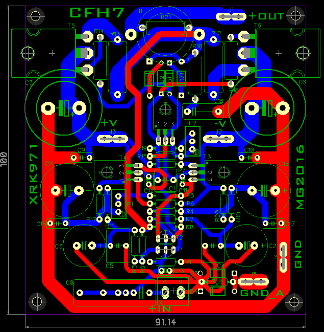
Is this the layout fromposthttp://www.diyaudio.com/forums/solid-state/294834-cfh7-amp-4.html#post4803910 173? It looks like the ground for the entire amp is attached through the ground lift at the input. First thing I would try is shorting that ground lift. If that works we can go from there.
I am indeed the first to build this layout shown below (the one prior to the one you reference where the ground bus loops in a U shape around the input stage). I shorted the ground lift between the power ground and signal ground FASTON tabs with solid 12 gauge copper wire soldered connection.
I did not run a separate ground wire to the PSU ground. Is this the ground after the rectifier or the earth ground before the rectifier? As I said, the DAC PSU is in grounded - connected via 120vac mains as same point as 120vac input to primary of the 250va 25vac toroidal trafo for power amp PSU.
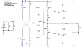
This is my amp:
It seems that there is a DC offset being imposed on the ground reference for the amp and this shifts the Vbe multiplier loop into action when DAC is connected.
It's almost like this amp needs a 1N4148 in series with one of the current supplies of the VAS stage to lift it up to a working voltage range.
Last edited:
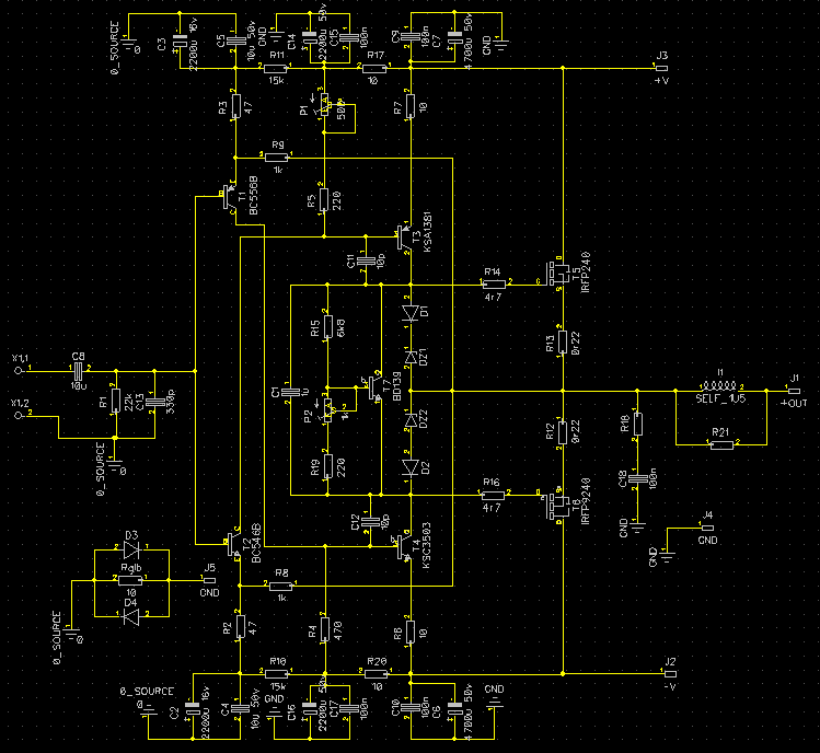
BC556B and BC546B as specified.
KSA1381 and KSC3503 for T3/4
Vishay IRFP240 and IRFP9240 for outputs.
KSA1381 and KSC3503 for T3/4
Vishay IRFP240 and IRFP9240 for outputs.
Last edited:
I am indeed the first to build this layout shown below (the one prior to the one you reference where the ground bus loops in a U shape around the input stage). I shorted the ground lift between the power ground and signal ground FASTON tabs with solid 12 gauge copper wire soldered connection.
I did not run a separate ground wire to the PSU ground. Is this the ground after the rectifier or the earth ground before the rectifier? As I said, the DAC PSU is in grounded - connected via 120vac mains as same point as 120vac input to primary of the 250va 25vac toroidal trafo for power amp PSU.
This is my amp:
It seems that there is a DC offset being imposed on the ground reference for the amp and this shifts the Vbe multiplier loop into action when DAC is connected.
It's almost like this amp needs a 1N4148 in series with one of the current supplies of the VAS stage to lift it up to a working voltage range.
The layout you use is bad...the one from post #194 i s much, much better.
To get your amp working first desolder a short and two anti-parallel 1N4148 diodes (10 Ohm resistor remains in place in both amp boards) between signal ground and power ground. Now, connect GND_A to GND, the amp should work now without a hum (each of left/right amp will still have a big ground loop, but all currents generated inside of each amp will be waisted on said 10R resistors.
Another thing... a 10R resistor in // with 2 anti // diodes (and/or capacitor) must be placed between amp power ground and earthing , not between signal ground and power ground!
Aparatusonitus (that was tough to spell on my phone - it kept trying to autocorrect it a hundred times):
You mean short D3 and D4? And tie the two ground pins J4 and J5 together?
I already removed D3 and D4 but replaced 10R with jumper so no resistor at all. Those diodes and resistor were suggested by Andrew T I think. As I mentioned earlier, J4 and J5 soldered together with 12mm long piece of low impedance 12 gauge solid copper wire. Anyhow, removing diodes and shorting 10R did nothing to help. I will put 10R ground lift resistor back sans two diodes.
This whole dual ground a la PeeCeeBee is a total mess - never had such problems until trying to do it now. All my previous amps had single ground connection from PSU and sometimes a 10R ground lift resistor for signal ground referenced to PSU ground.
Should I cut the big ground U trace to break up the loop and replace with a short thick gauge wire around the top of the board like second layout?
Last edited:
What schematic are you using to populate this board? The one I have has some different part numbers from what are on the board. Could it be you have some values in the wrong places?
I am using the one from
Idefixes for generating the layout so it's 1:1 correlation.
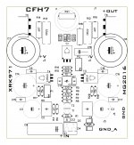
Layout again for convenience to see next to each other:
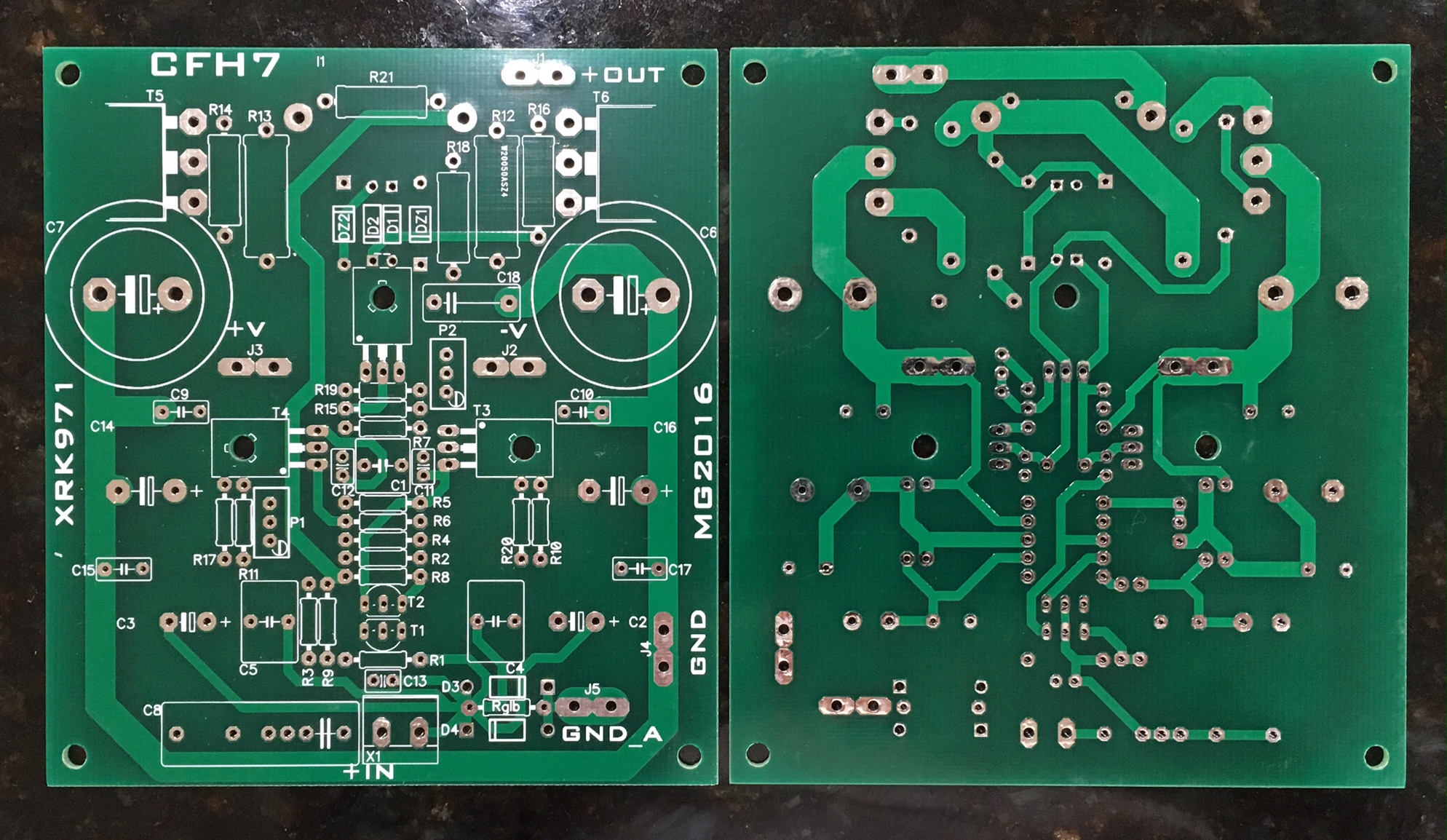
And PCB as-manufactured from Gerber of above:
Just want to let you all know I appreciate all the help and time you are giving me to look at this. Hopefully we will get it cleared up and it will be something simple like just removing those two diodes or cutting trace and replacing with external ground bus.
Idefixes for generating the layout so it's 1:1 correlation.
Layout again for convenience to see next to each other:
And PCB as-manufactured from Gerber of above:
Just want to let you all know I appreciate all the help and time you are giving me to look at this. Hopefully we will get it cleared up and it will be something simple like just removing those two diodes or cutting trace and replacing with external ground bus.
Last edited:
Well if you shorted the ground lift resistor and connected both Ground lugs then that is not the problem. It may not be the best for noise but all of the ground points are connected to ground so the amp should work. My amp works so we know the circuit works. I'm attaching a silk with the values inserted for easy checking. Also make sure you have the correct value for the trimmers. I got bit by that last week on a different amp. With the amp powered up, measure the base-emitter voltages of T3, T4 and T7. Should be about 0.6V each. Easy measurement because it is the two outer legs.
If you are not getting enough current at the output then the feedback will not work, so we have to find out why you can't adjust the bias.
I don't mind helping if I can. I learn from this too. If an amp works right off the bat I usually don't learn anything. 😀
If you are not getting enough current at the output then the feedback will not work, so we have to find out why you can't adjust the bias.
I don't mind helping if I can. I learn from this too. If an amp works right off the bat I usually don't learn anything. 😀
Attachments
Thanks, Terry.
I will do the base-emitter voltage measurement when I get home. Thanks for the silk screen layout. I went through the resistors last night and have everything correct I think. A few 'close-enough' substitutions due to lack of supplies: 1k was made with two 470R in series for 940R, 15k was made with two 6.8k in series for 13.6k. I don't think those should affect the problem areas I am facing. I did double check the pots and even changed them for fear of an internal fault. 500R on offset and 1k on bias adjust.
I will do the base-emitter voltage measurement when I get home. Thanks for the silk screen layout. I went through the resistors last night and have everything correct I think. A few 'close-enough' substitutions due to lack of supplies: 1k was made with two 470R in series for 940R, 15k was made with two 6.8k in series for 13.6k. I don't think those should affect the problem areas I am facing. I did double check the pots and even changed them for fear of an internal fault. 500R on offset and 1k on bias adjust.
Aparatusonitus (that was tough to spell on my phone - it kept trying to autocorrect it a hundred times):
Yes i know...forum rules prevent me to put one more π in my nick...call me Ivo from now on😉
Those diodes and resistor were suggested by Andrew T I think.
It may be so, but Andrew knows about grounding and for sure knows where and how to put a ground insulator.
This whole dual ground a la PeeCeeBee is a total mess - never had such problems until trying to do it now. All my previous amps had single ground connection from PSU and sometimes a 10R ground lift resistor for signal ground referenced to PSU ground.
It is not a mess...it's perfectly legit and good practice...allows you different ways of grounding depending on the source and amp psu...are they powered from single psu (troubles arises) or dual mono psu (each channel have its own psu)
Should I cut the big ground U trace to break up the loop and replace with a short thick gauge wire around the top of the board like second layout?
One step at a time...get the amp working as it should🙂
Btw, Vbe multipier (as it is) will actually overcompensate for any bias current...I predict. A quick fix - put a resistor in series with bias transistor emitter. Optimal solution would be Vgs multiplier with the same geometry as output m-fets (think IRF620/630/640 instead BD139) with bias resistors/trimmer values recalculated. Moreover, you would not need any source resistors on output M-fets as long as only a single pair of complementary m-fets are in use in ouput like IRFP240/IRFP9140 up to +/-40VDC, or IRFP340/9240 up to +/-80VDC.
Ivo,
I have one toroidal power trafo but dual PSU rectifier/caps/filters one for ea amp. The BD139 has been mentioned by someone else as overcompensating when used with IRFP240/9240 (in FH9/FH11/12 Apex thread). But I have used it many times and slower lag of heatsink thermal mass and the overcompensation seems to work out just fine. It has been very stable in the past with the 6.8k/1k pot/220R Vbe arrangement.
I hope I can salvage these boards and get them working.
Thanks,
X
I have one toroidal power trafo but dual PSU rectifier/caps/filters one for ea amp.
Ok, then you don't need 10R resistors at all, as well as anti-parallel diodes at amp boards.
Ground the amp input and measure all circuits nodes voltages and stick them on your schematic so anyone can see what is going on.
Btw, Vbe multipier (as it is) will actually overcompensate for any bias current...I predict. A quick fix - put a resistor in series with bias transistor emitter. Optimal solution would be Vgs multiplier with the same geometry as output m-fets (think IRF620/630/640 instead BD139) with bias resistors/trimmer values recalculated. Moreover, you would not need any source resistors on output M-fets as long as only a single pair of complementary m-fets are in use in ouput like IRFP240/IRFP9140 up to +/-40VDC, or IRFP340/9240 up to +/-80VDC.
Resistor will not change the bias spreader tempco, better use a LED, I think red one could be good.
By the way Ivo, why do you think IRFP340/9240 are beter complements then IRFP240/9240, I don't see it from the datasheets. Forward transconductances are even further apart.
Damir
As I said...a quick fix...LED is very good, even a simple signal diode would make a better bias stability. But the best one is achieved with Vgs multiplier...almost no change in OS bias (like few mA) from cold to fully warm up amp.
Regarding complements...tell me what you see from fig.1 and fig.2 from datasheet of IRFP340/9240 and fig.5 as well as data for Ciss, Coss Crss from table against IRFP240/9240 combo?😉
Regarding complements...tell me what you see from fig.1 and fig.2 from datasheet of IRFP340/9240 and fig.5 as well as data for Ciss, Coss Crss from table against IRFP240/9240 combo?😉
Well if you shorted the ground lift resistor and connected both Ground lugs then that is not the problem. It may not be the best for noise but all of the ground points are connected to ground so the amp should work. My amp works so we know the circuit works. I'm attaching a silk with the values inserted for easy checking. Also make sure you have the correct value for the trimmers. I got bit by that last week on a different amp. With the amp powered up, measure the base-emitter voltages of T3, T4 and T7. Should be about 0.6V each. Easy measurement because it is the two outer legs.
If you are not getting enough current at the output then the feedback will not work, so we have to find out why you can't adjust the bias.
I don't mind helping if I can. I learn from this too. If an amp works right off the bat I usually don't learn anything. 😀
With inputs shorted. T3 and T4 B-E are 0.60v and T7 B-E is 0.36v. G on IRFP240 is 1.38v relative to GND, G on IRFP9240 is -3.00v. Output DC offset is 0mV. 0mV across R12 and R13 (0.22R).
Rails are at +/-36.0v.
So what does it mean for B-E on Vbe multiplier to only be 0.3v? The pot is at some intermediate position that allows 180mA of bias when DAC is connected.
With DAC connected T3 BE is 0.44v and T4 BE is 0.6v. T7 BE is 0.6v. Output is 1.1v DC offset. Input is 0.225v DC.
Last edited:
The layout you use is bad...the one from post #194 i s much, much better.
To get your amp working first desolder a short and two anti-parallel 1N4148 diodes (10 Ohm resistor remains in place in both amp boards) between signal ground and power ground. Now, connect GND_A to GND, the amp should work now without a hum (each of left/right amp will still have a big ground loop, but all currents generated inside of each amp will be waisted on said 10R resistors.
Another thing... a 10R resistor in // with 2 anti // diodes (and/or capacitor) must be placed between amp power ground and earthing , not between signal ground and power ground!
Aparatusonitus (that was tough to spell on my phone - it kept trying to autocorrect it a hundred times):
You mean short D3 and D4? And tie the two ground pins J4 and J5 together?
I already removed D3 and D4 but replaced 10R with jumper so no resistor at all. Those diodes and resistor were suggested by Andrew T I think. As I mentioned earlier, J4 and J5 soldered together with 12mm long piece of low impedance 12 gauge solid copper wire. Anyhow, removing diodes and shorting 10R did nothing to help. I will put 10R ground lift resistor back sans two diodes.
This whole dual ground a la PeeCeeBee is a total mess - never had such problems until trying to do it now. All my previous amps had single ground connection from PSU and sometimes a 10R ground lift resistor for signal ground referenced to PSU ground.
Should I cut the big ground U trace to break up the loop and replace with a short thick gauge wire around the top of the board like second layout?
I had the inverse parallel diodes between the Main Audio Ground and Chassis. The diodes pass FAULT current to PE if the circuit ever comes into contact with the mains.As I said, remove completely (not only short them!) D3/D4 and remove a short over 10R.
I did not have inverse parallel diodes between Signal Return and Speaker Return. It was another Member that showed this modification and I "clicked". This is another route for FAULT current to pass to PE and blow a fuse if the input wiring should ever come into contact with the mains. Now the circuit was safe.
I have recommended that dual inverse parallel diodes since that revelation.
You NEED the SAFETY diodes if you fit the HBRR/HBRL between Signal Return and Speaker Return.
The signal current that flows from, or to, this voltage reference is miniscule. Try measuring the voltage across the 10r.
If however there is a big interference voltage between SOURCE and RECEIVER then you will get a big voltage across the 10r. To cure this you connect the two Chassis with a big flat copper braid. H.Ott makes that very clear in his writings.
I didn't have anymore time to work on this amp last night. I am still puzzled what it is about the layout that is giving me problems though. In theory it seems like it should all work. Still puzzled by why connecting the DAC to an AC coupled audio input would shift the DC offset of the Vbe multiplier circuit and put it in a range that flows current. I think this must be some sort of AC coupled oscillation phenomena as AndrewT suggests. Perhaps my little cheap 10pF caps between C-B of the KSC//KSA's is insufficient to suppress oscillation? But isn't oscillation usually shown by unstable bias current? Or at least some bias rather than the OPS shutting down.
I have a 330pF RF block to ground on the input pin. Isn't that usually sufficient to prevent RF from getting trough? It's a virtual short at high frequencies.
I don't know what HBRR/HBRL stands for?
I have a 330pF RF block to ground on the input pin. Isn't that usually sufficient to prevent RF from getting trough? It's a virtual short at high frequencies.
I don't know what HBRR/HBRL stands for?
- Home
- Amplifiers
- Solid State
- CFH7 Amp