for a Low pass filter you need both parts of RC or LC.
You don't have a defined R .
You are relying on the output impedance of the DAC and the inductance of the interconnect.
You need to sort the RF filter at the input and then see what needs investigating.
It might be nothing to do with injecting excessive HF into the input, but it is simply good practice to use the two passive input filters.
Read D.Joffe for an explanation of interference in a stereo amplifier when you connect TWO or more interconnects to an amplifier.
He suggests adding HBRR & HBRL to attenuate the interference current that flows around the screens of the two coupled interconnects.
Last edited:
Most amplifiers work well.
Most properly working amplifiers that have identical frequency response sound the same when not overloaded and not abused.
Most amplifier problems are associated with the way we wire them up. That mis-wiring is usually the cause of all the "problems" and lack of sound quality in the assembled amplifier system.
One needs to get the amplifier working without all those wiring problems that are corrupting the sound. Then one can assess the amplifier.
You will find that almost all of my constructive comments are directed towards eliminating or reducing the effects of that mis-wiring or locating components in the wrong place. I rarely comment on the "amplifier" and that's because I am not an amplifier Designer.
Last edited:
Ok, if I add 2k2 resistor between the 10uF input cap and the 330pF RF filter cap that should give about 2MHz RF filter frequency based on 0.7RC.
I am also thinking my 10pF ceramic caps may be problematic. They have no voltage rating and are tiny. Perhaps they are just plain bad and may even act like a short at RF so the collector-base junction on the drivers are semi- shorted. Will look for proper NP0 caps - might be a larger value while I wait for good ones to arrive from Digikey.
I am also thinking my 10pF ceramic caps may be problematic. They have no voltage rating and are tiny. Perhaps they are just plain bad and may even act like a short at RF so the collector-base junction on the drivers are semi- shorted. Will look for proper NP0 caps - might be a larger value while I wait for good ones to arrive from Digikey.
2MHz is far too high.
40kHz is probably too low but will remove more RF than a 200kHz filter.
One usually sees an RC time constant between 200ns (800kHz) and 2000ns (80kHz) that effectively attenuates RF and lets through all the audio frequencies.
Some will argue that even that restricted range is too narrow and prefer to make the window even wider open.
If your DAC passes higher levels of RF, then you may need to consider a more severe filter, but you do need to check what HF performance your extra opamp would require to act as an effective RF filter at the highest frequencies. That the beauty of passive . If you use an smd cap at the input socket of the receiver you have almost no inductance and the cap attenuates to VHF.
Have you noticed that I often recommend adding a 47pF at the socket, as well as the amplifier filters?
BTW,
2k2 & 330pF = 726ns and that equates to F-3dB = 219kHz
Last edited:
Hmm... Tau=0.7RC, f=1/(0.7RC). Is my equation wrong?
I get 1.97MHz still for 2200ohms and 330pF. Anyhow it seems to be a typical combo used in many amp in the Apex lineup. I agree maybe more severe circa 400kHz would be better.
Are you saying 47pF SMT soldered between input pin and ground - no resistor?
I get 1.97MHz still for 2200ohms and 330pF. Anyhow it seems to be a typical combo used in many amp in the Apex lineup. I agree maybe more severe circa 400kHz would be better.
Are you saying 47pF SMT soldered between input pin and ground - no resistor?
For a single pole Low Pass Filter:
F=3dB = 1 / {2 Pi R C}
The RC part is the time constant.
2Pi does not equal 0.7 !
1/{2*3.142*2200*330p} = 219kHz
SMD cap soldered between the hot lead and the barrel across the tiny gap that is filled with insulation.
Better would be a ring of tiny smd fanning out around the hot pin. Holding them in place while you melt in the next one would be a problem. A pair of 603, or 402, caps 10pF to 22pF would do.
Second best would be a leaded cap with the leads cropped to about 1.5mm long, shaped and soldered across that gap using the shortest possible leads.
Last edited:
XRK, you have something wrong. The circuit works. You have a bad connection, wrong value resistor or bad transistor. Don't change the circuit until we find what is wrong. Please take a little time and mark up a schematic with voltages at each leg of each transistor. Make sure the input is shorted. There will probably be more questions but at least that will give us a chance to help find the issue.
For a single pole Low Pass Filter:
F=3dB = 1 / {2 Pi R C}
The RC part is the time constant.
2Pi does not equal 0.7 !
1/{2*3.142*2200*330p} = 219kHz
SMD cap soldered between the hot lead and the barrel across the tiny gap that is filled with insulation.
Better would be a ring of tiny smd fanning out around the hot pin. Holding them in place while you melt in the next one would be a problem. A pair of 603, or 402, caps 10pF to 22pF would do.
Second best would be a leaded cap with the leads cropped to about 1.5mm long, shaped and soldered across that gap using the shortest possible leads.
My confusion comes from the 1/e RC discharge time constant. You would think they would be similar and not 10x different!
XRK, you have something wrong. The circuit works. You have a bad connection, wrong value resistor or bad transistor. Don't change the circuit until we find what is wrong. Please take a little time and mark up a schematic with voltages at each leg of each transistor. Make sure the input is shorted. There will probably be more questions but at least that will give us a chance to help find the issue.
Will do. I need to put shrink tube on the DMM probe tip to avoid exposing the main shaft as my clumsy hands have burned more than some parts from poking around with an exposed tip.
It's like Aksa said, "be careful when you drive the car through the garage door." 🙂
What I will do often is to look at the trace layout and use a connected resistor leg as a probe point rather than try to get the probe into the legs of a TO-92. Another thought came to mind. Did you have to drill out any holes to make a part fit? If so, it is possible that you drilled out the through plating. If so you need to make double sure that you have the lead soldered top and bottom.
.....SMD cap soldered between the hot lead and the barrel across the tiny gap that is filled with insulation.
Better would be a ring of tiny smd fanning out around the hot pin. Holding them in place while you melt in the next one would be a problem. A pair of 603, or 402, caps 10pF to 22pF would do.
Second best would be a leaded cap with the leads cropped to about 1.5mm long, shaped and soldered across that gap using the shortest possible leads.
Interesting stuff nowadays with all these transmitters around us.
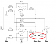
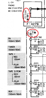
Have a couple of Behringer devices that use 100pF as in below attachments at input but also at output which guess is to protect RFI into OPA feedback network. Last attachment is Sansui amp from nineties it use 1uf with short wires on floating phono sockets ground directly to chassis for normal line level inputs and 47nF for phono socket.
Attachments
Neat stuff Byrtt. Maybe I am plagued by RF interference? Funny how Terry's amp (and I assume AndrewLebon) worked just fine without issues.
Hi Terry,
Yes, I did drill out screw holes on three TO-126 and yes, I checked to make sure no traces got harmed in the process. It was close to one trace but not impacted.
Thanks for the question though.
Did you have to drill out any holes to make a part fit? If so, it is possible that you drilled out the through plating. If so you need to make double sure that you have the lead soldered top and bottom.
Yes, I did drill out screw holes on three TO-126 and yes, I checked to make sure no traces got harmed in the process. It was close to one trace but not impacted.
Thanks for the question though.
Hi Terry,
Yes, I did drill out screw holes on three TO-126 and yes, I checked to make sure no traces got harmed in the process. It was close to one trace but not impacted.
Thanks for the question though.
I was referring to drilling out device pin holes.
Still waiting to see a schematic with measurements. Without that we are all just guessing.
With inputs shorted. T3 and T4 B-E are 0.60v and T7 B-E is 0.36v. G on IRFP240 is 1.38v relative to GND, G on IRFP9240 is -3.00v. Output DC offset is 0mV. 0mV across R12 and R13 (0.22R).
Rails are at +/-36.0v.
So what does it mean for B-E on Vbe multiplier to only be 0.3v? The pot is at some intermediate position that allows 180mA of bias when DAC is connected.
With DAC connected T3 BE is 0.44v and T4 BE is 0.6v. T7 BE is 0.6v. Output is 1.1v DC offset. Input is 0.225v DC.
You definitely have a problem here as Terry notes.
If you have 0.36 across T7 BE it means that it is OFF.
You are measuring 0V across the 0.22 Ohm resistors - which means that the output mosfets are also OFF so we can assume from this that the voltage across the CE of T7 is below the output mosfet threshold.
If T7 is OFF, normally I would expect T3 and T4 to pull the gates of the mosfets up to their respective rails and very high current to flow in the output devices.
However, this is not happening, so we can assume that little of no current is flowing from T3 to T4. You can confirm this by measuring the volt drop across R4 and then across R5+P1 - in both cases should be 0.6V or thereabouts. Check the values of R6 and R7 - if one of these is open, or a high value, you would have problems similar to the one you are seeing.
If the bases of T1 and T2 were not connected to 0V, then you would still measure 0.6V BE voltage but they would not be conducting enough to turn the 2nd stage devices on fully. When you connect your DAC, you are probably providing a path to ground through the cap leakage, or simply via capacitively coupled noise which is enough to get the amp partially biased up.
I would also carefully check that R1 is OK and that there is a good connection between the bases of the input devices to R1 - i.e. track not broken or resistor open or a very high value.
You should focus on getting the DC bias conditions correct before addressing any potential noise issues IMV.
 DIY at full throttle
Thanks Bonsai. Those are very helpful comments/tips to check. I did not get a chance to work on it yesterday except go grab a few voltages that Terry asked for on the E-B pins of the transistors. I am suspecting that I have a mistake in the resistors based on my photo. I originally thought I did not have 470R so replaced with 510R but then switched them to proper 470R later after the photo. However I think I have a big error in placement - so I may have 470R instead of 10R at R6 position. Seems like a big easy mistake to spot but problem was I wrote down the wrong value on my stuffing guide. So when double checking it looks good. It wasn't until Terry posted the silk and you mentioned to look at R6 and R7 that I realize from memory this maybe the case. That's my whole issue with PCBs labeled generically. You really need an accurate BOM/stuffing guide - whereas I generated mine from the schematic on a napkin. 😀
I tried checking the resistors from your picture but between lighting, camera and them computer display, colors are not always what they seem. Hopefully you get it worked out. It would be nice if you could hear your creation.
R6 was indeed incorrect at 470R vs specified 10R. I replaced it and bingo, amp works now. Bias is easily set and DC offset is easily set with inputs grounded. Not much time to listen buy for 2 tracks and they sound wonderful. No distortion. Deep powerful bass.
Thanks to everyone for helping. It was a total boneheaded mistake.
Idefixes - your layout is fine and works great!
Mea culpa. My apologies for wasting everyone's time helping me.
Thanks to everyone for helping. It was a total boneheaded mistake.
Idefixes - your layout is fine and works great!
Mea culpa. My apologies for wasting everyone's time helping me.
CFH7 in Stereo
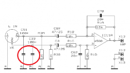
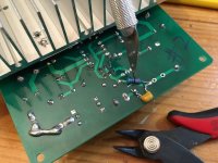
The amp is playing nicely with the DAC now that I added a 2k2 resistor between the 10uF input cap and the 22k resistor to ground. I cut the trace with an xacto then soldered the 2k2 resistor on the underside. This seems to have cured the instability it gets when connected to the RF noisy DAC. I wonder if this will allow me to use 4.7R gate stoppers per the original design?
Anyhow, here is a photo of the 2k2 filter mod:

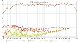
Here is the measured response with harmonic distortion, the distortion at the speaker is low - on a par with the other amps. The response appears to be flatter frequency than the other amps. however, the mic was moved and replaced in the same spot (based on height above floor and distance from baffle), but not "untouched" like previous measurements. The sound is very balanced, dynamics are excellent, and imaging and sound stage are very nice:

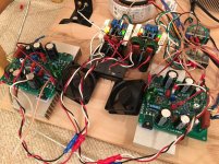
Here is the setup in stereo:

I have recorded comparison sound clips in the other virtual audition thread.
The amp is playing nicely with the DAC now that I added a 2k2 resistor between the 10uF input cap and the 22k resistor to ground. I cut the trace with an xacto then soldered the 2k2 resistor on the underside. This seems to have cured the instability it gets when connected to the RF noisy DAC. I wonder if this will allow me to use 4.7R gate stoppers per the original design?
Anyhow, here is a photo of the 2k2 filter mod:
Here is the measured response with harmonic distortion, the distortion at the speaker is low - on a par with the other amps. The response appears to be flatter frequency than the other amps. however, the mic was moved and replaced in the same spot (based on height above floor and distance from baffle), but not "untouched" like previous measurements. The sound is very balanced, dynamics are excellent, and imaging and sound stage are very nice:
Here is the setup in stereo:
I have recorded comparison sound clips in the other virtual audition thread.
Attachments
Last edited:
- Home
- Amplifiers
- Solid State
- CFH7 Amp