That file has been computationally pruned of obviously bad models, but it still includes a lot of models that probably haven't been tested. I would use it as a last-ditch lib if a transistor wasn't in my kean.bjt library.
. . . This also brings up a problem with the idea of having a discrete driver for each output. The drivers themselves in this case will add to the differential thermal runaway.
. . .
My interest with lowering emitter resistors is to allow the 13mV bias point without sacrificing Ft with low bias. The 13mV bias point could have the same first-watt THD as a GM-doubled bias point, but they would have odd order harmonics of the opposite polarity. For this reason I suspect the low bias point may sound better and be more economical.
Drivers adding to thermal runaway?
Lower bias point may sound better?
Totally logical; however, I'd sure like to know or hear something about it.
Drivers adding to thermal runaway?
If you have a pair of drivers for each pair of outputs, you are at greater risk for current hogging. You can reduce this risk if you put all the same-side drivers close to each other on a separate heatsink.
Lower bias point may sound better?
The resistor voltage matters most directly for harmonic profile. 12mV with 0.22R will have the same harmonic profile as 12mV with 0.33R, the main difference that the higher current bias will have a larger class A region and higher Ft. This is as long as the transistors are behaving mostly intrinsically. In Pavel's graphs, something seems different, because usually I see a more wiggly transition there.
At any rate, I messed up the thermal conductivity units for the last graph, so here is a new one.
Attachments

Okay, I didn't understand your graph at first because you used a sweep and I just use sines.
Notice that between 7.5mV and 15mV you have curves pointing different directions. At ~12.5 mV the curves balance out to a linear region rather than convex or concave.
You should add that cause it's worth showing - only in deep Gm doubling is there another bias point where the first watt is this linear AFAIK.
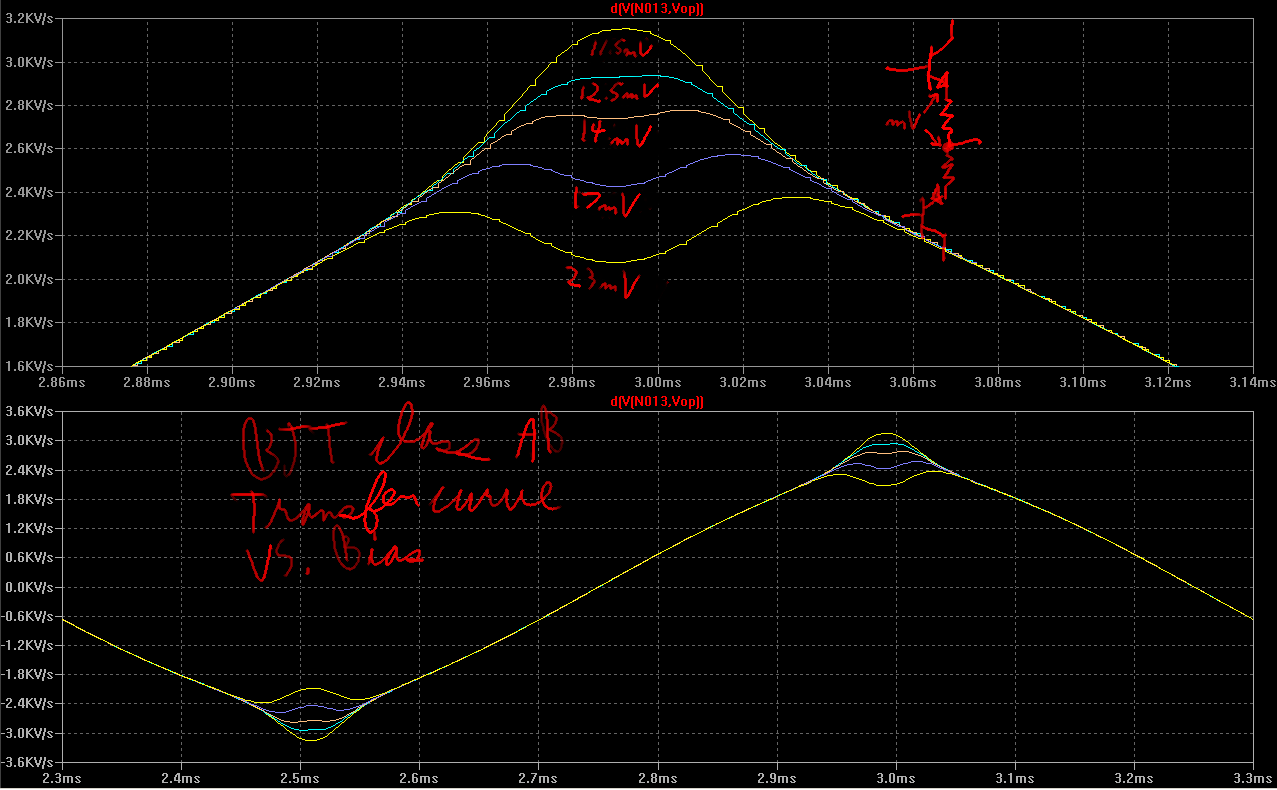
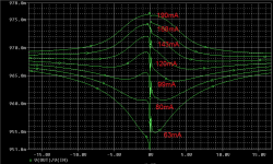
Output stage (MJL1302/3281) + driver only, 4 pairs of output devices, transfer function vs. idle current. Re = 0.22
- Simulation, right?
- RE, RB, BF in the models?
- Load?
- yes
- 0.00127227, 11.988, 139.247
- 8
RB=12 ohm adds 0.1-0.2 ohm to the equivalent RE, depending on BF(IC). No wonder the optimal bias current is so low. I don't think 12 ohm is anywhere close to reality. My MJE1302 model has RB=3.3ohm.
Let me elaborate: I have found that it is possible to operate power amps with as little as 0.05 ohms successfully, however this is for a single pair of complementary devices. When you SHARE current with multiple devices, then a second problem appears, this is thermal 'hogging' by some devices, leading to thermal runaway.
The formula for optimum transition from Class A to Class B is still valid, but it is difficult to have more than a certain amount of standing current for each device without a somewhat larger Re in each device. This smooths out the differences between different parts of the heat sink characteristics and uneven beta (which can be removed by close matching). The JC-1 power amp DID have some problems with 0.1 ohm resistors, however with 0.15 ohm resistors, and close beta matching, we have been able to make many hundreds of this design without any further problem. IF we were forced to use 0.22 ohms, then we would be forced to use about 0.1A per transistor and this would reduce the Class A standing current to below our design goal of 25W into 8 ohms.
To increase this current further would cause a 'bump' in the transfer function that would be less than optimum.
Hi John,
The fact that you had serious enough thermal stability problems in the JC1 to go up to 0.15 to get adequate amplifier thermal stability indicates that you were way beyond the point already where thermal issues during program material were moving you way away from optimum bias. That sort of thing happens long before you lose control of thermal stability to the point where you have to change the design to keep it safe.
That having been said, I do like the concept of having as much class A operating range as possible, but going to very low values of RE (and having large values of base stoppers, as I recall you did) is not the way to go.
We each pick our own poison.
Cheers,
Bob
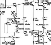
OS, First I tried my CFA and burned 2 feedback resistor 😱. And then I choose to finish my VFA. But right now, I can made my CFA singing 😎. I listening one VFA and one CFA in stereo 😀.
I develop test procedure to each module before they connected.
For OPS, I use your suggestion to put 2 resistor to simulate VAS current.
FOR IPS, I just connect VAS+ output, VAS- output, and Feedback.
I found designing CFA is more challenging than VFA.
I will try many IPS topology.
Yes , the CFA has a higher "learning curve". This is why I chose the VFA
"blameless" (Badger) for DIYA's amp ... many builders are first timers from
the pass and tube amp "camps".
The goal of having a nice platform (the HK EF3) has succeeded. You and thimios are porting the ef3 for MJE15032/33 and smaller wattage. It's
about time the forum moved beyond overloaded EF2's ! EF3 ...all the way.
For CFA , the basic VSSA is an amazing thing (below 1). I backed off the bloated
CM method for better PSRR and went "KISS" for the VSSA. Bypassing the
VAS and using just the simple LED CCS , I was able to compromise to
90db PSRR with VERY few devices.
The VSSA is both better at LF THD and Offset using only a slight trim of one of the CCS's to get mV offset and the 2 DC caps.
Mr. Marshes concern of LT vs. real amp performance is noted. Why would
all the operating points be within mV and uA on the real thing ... but the other metrics be way off ?
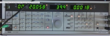
Member ASTX , with his 20K$ analyzer (below 2) ... shows my blameless at the same
20K thd as I simulate it (his is VERY similar). So , I don't think we are too far
off.
PS - Bimo ... how do you run a CFA IPS in isolation ? The VAS would not have the
current to develop the feedback without the OPS ... ?
OS
Attachments
Last edited:
Let us not confuse details and personal opinion with what works. There is NO perfect fit, just a 'best fit' and that may be the difference between extra low measured thd distortion and lower high order distortion.
Agreed. The crossover region often involves enough non-idealities and subtleties that the "ideal" 26 mV biasing theory is only a starting point. There are many different tradeoffs here where individual design preferences may also come into play.
Cheers,
Bob
I suspect the bias is not set low because of power dissipation, but because of bias creep as temp rises. Most heatsinks will easily cope with 50 mA per pair idle dissipation vs say 20 mA (that's low power in the context of things) so what's the point then of setting it at some much lower figure as we typically see? The reason is as the amp warms up, the bias increases such that at normal operating levels after 30 mins or so, the bias is about right. This is what I call single slope temperature compensation. Where it actually settles, and what assumptions are used are a matter of choice on the designers part.
The idea is to get the ideal current and temperature to intercept at 2 points, rather than 1 point, by design rather than luck. I wrote up my thoughts on this a few years ago after working on my original 250 Watt EFT amplifier from 2007/7. On a later design, the e-Amp, I used an NTD to basically do the same thing.
Most bias schemes are single slope and when you read Self's or Bob Cordell's on this specific subject, you can see it is an exercise in compromise rather than a solved problem.
For EFT, I am an advocate two slope or two point thermal comp, which seems to improve things markedly i.e. the bias current is much more stable over a wider junction temp - the Thermaltrak devices are also an attempt and a useful tool to solve this problem. The issue is much less of a problem on EF2's - EF3's are an entirely different matter though.
Some Ideas on Temerature Compensation for Audio Amplifier EF Triples
Yes, EF3's are a more difficult problem, mainly because the pre-driver and/or the driver are not always mounted on the main heatsink, so thermal compensation for their Vbe changes with temperature is not properly taken care of by a single Vbe multiplier transistor mounted on the main heat sink. One solution I suggested in my book is to mount both the predrivers and drivers together on the same, separate heat-spreader/heat sink on the board, and have a second Vbe multiplier temperature sensor for them. This makes the secondary temperature compensation for the drivers/pre-drivers easy and stable, especially since they are usually in class A. These linds of techniques can also be used with other types of triples, such as the diamond buffer triple.
Cheers,
Bob
RB=12 ohm adds 0.1-0.2 ohm to the equivalent RE, depending on BF(IC). No wonder the optimal bias current is so low. I don't think 12 ohm is anywhere close to reality. My MJE1302 model has RB=3.3ohm.
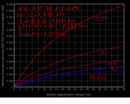
This is what I get with my models (optimum at around 22mV across Re). Bottom line, these simulations are relying way to much on unknown (or grossly estimated) parameters to be reliable. Hence, in general, predicting by simulation the distortions in bipolar output stages is at best iffy if not outright wrong. You can of course analyze relative results (rather than absolute results).
This (distortion modeling) is an area where mosfets have a slight advantage, lacking the bipolar gm doubling effects, the distortions are more predictable (down to, or up to, the missing subthreshold conduction models).
Attachments
12 ohms, or 10 ohms for a base stopper is ridiculous. Something below 5 is much more like it and a ferrite bead is probably ideal ( I need to play with this option and get a feel for its effectiveness though in a practical class AB)
Yes, EF3's are a more difficult problem, mainly because the pre-driver and/or the driver are not always mounted on the main heatsink, so thermal compensation for their Vbe changes with temperature is not properly taken care of by a single Vbe multiplier transistor mounted on the main heat sink. One solution I suggested in my book is to mount both the predrivers and drivers together on the same, separate heat-spreader/heat sink on the board, and have a second Vbe multiplier temperature sensor for them. This makes the secondary temperature compensation for the drivers/pre-drivers easy and stable, especially since they are usually in class A. These linds of techniques can also be used with other types of triples, such as the diamond buffer triple.
Cheers,
Bob
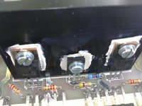
In my TT amp I fixed Vbe transistor on the same heath sink with the drivers, and TT diodes take care of output transistors, result, very small thermal drift.
BR Damir
by the way REs are 0,16 ohm
Attachments
PS - Bimo ... how do you run a CFA IPS in isolation ? The VAS would not have the
current to develop the feedback without the OPS ... ?
OS
I just want to measure DC operating point when I try my design. If I am sure the DC operating point is correct, then I connect the IPS and OPS. After that I connect the output to oscilloscope to see any indication of oscillation or not. Then I am connecting the dummy load and signal generator.
Attachments

Last edited:
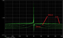
Another of my ignorant question here. Is the chart that Waly just posted indicative of the crossover distortion that I read about here going from class A to class AB? Is this where we are crossing over the X axis and see the swing in direction?
I have 100's of large power amps out in the public that work just fine. OF COURSE, a larger emitter resistor makes building easier (and potentially sloppier) but 0.22 is NOT necessarily the optimum value for ALL high power amps.
Now, when designing the JC-1, I DID run into problems and I changed from 0.1 to 0.15 because of manufacturing irregularities that I could not control, BUT 0.1 would work if I were in charge of matching and the heatsink.
Bob I wish to commend you about the problem using too high a a base stopping resistance. For the last 30+ years, starting with the introduction of high F(t) output transistors from Japan, I have used 10 ohm resistors as a default value, as suggested by the late Jon Everson, back in 1980 or so. However, your criticism of my choice led me to mathematically re-evaluate that decision and I have suggested a somewhat less value to Parasound recently, but as you know, we must not use too low a resistance, or we will not cancel the -R that can be created by a follower and a capacitive load sometimes. I LIKE Class A, so I start with what heatsink that is available for the project, then run the devices to about 50 degrees at Idle, or so, then choose the Re to go with it. I have almost 30W (into 8 ohms) Class A available in the JC-1. I would make it 50 or more watts if I could.
Another of my ignorant question here. Is the chart that Waly just posted indicative of the crossover distortion that I read about here going from class A to class AB? Is this where we are crossing over the X axis and see the swing in direction?
That is a very good question.
When the OPS is under biased (relative to the Oliver optimum point), the OPS gain curve looks like a valley. That's an indication that the switching distortions are dominant.
When the OPS is over biased (relative to the Oliver optimum point), thed OPS gain curve looks like a ridge. That's an indication that the Gm doubling distortions are dominant.
Based on a gain curve visual derivative (the valley slopes seem more abrupt compared to the ridge slopes), we can estimate that the switching distortions will be much richer in high order distortions, one more good reason for the usual practice to slightly over bias the OPS.
Now, what's happening if we further increase the OPS bias? Take a look at the attachment. The ridge flattens out,that is, the gm doubling distortions are decreasing when we advance towards Class A. Ignore the center discontinuities that's a simulation artifact due to close to 0/0 numerical indeterminations.
So, when starting from Class B (zero bias) and advancing towards Class A, the OPS distortions are initially high and rich in high harmonics, they decrease toward the Oliver optimum Class AB bias point, they increase again over the Oliver optimum Class AB bias point, then they decrease again, in Class A, theoretically down to zero (at infinite bias current).
Attachments
I just want to measure DC operating point when I try my design. If I am sure the DC operating point is correct, then I connect the IPS and OPS. After that I connect the output to oscilloscope to see any indication of oscillation or not. Then I am connecting the dummy load and signal generator.
Is this what you are using ?
I see you use Jfet CCS's , and run the Cascode "HOT" .
I forgot the french designer ... but he also used the "magic" 4.7R between
active and cascode....
aaaah .. google found it - Memory Distortion Philosophies - Part 5 : Circuits, continued
"brainwashing the VAS" 😀 funny !
He never envisioned this for a CFA.
Does it "sing" ?? 🙂
OS
- Home
- Amplifiers
- Solid State
- CFA Topology Audio Amplifiers