There is a huge amount of distortion cancellation methods published onto the Internet using CMOS and low voltage operation. Some of those concepts or topologies can be adapted and use jFEt or bjt and higher voltages.
View attachment CMOS-LNA-noise-distortion-cancellation.pdf
Thx-RNMarsh
View attachment CMOS-LNA-noise-distortion-cancellation.pdf
Thx-RNMarsh
Last edited:
Replace all those CCS with complimentary transistors and you are right back here.
THx-RNMarsh
Thank-you Mr Marsh. I see your point, the symmetrical version is actually simpler. The appeal for me was thermal stability, no matching issues, SE harmonic structure and the speed of CFA. Well thats what I thought anyhow.
Yes most used EC at RF amplifiying is non feedback (as for LNA is modulating), it will be difficult to implement non feedback in class AB.There is a huge amount of distortion cancellation methods published onto the Internet using CMOS and low voltage operation. Some of those concepts or topologies can be adapted and use jFEt or bjt and higher voltages.
View attachment 385322
Thx-RNMarsh
PS: My simplest EC work in class AB with less sonic effect compared to halcro's. Ofcourse THD is not as low as halcro's. There are another thingy than just how to reach 1ppm THD. I am currently not using EC anymore.
Last edited:
I am currently not using EC anymore.
Probably because of its little benefit to the sound quality, if any, not because of the circuit complexity?
Probably because of its little benefit to the sound quality, if any, not because of the circuit complexity?
Yes, because I care the sound more.
When my wife (instead of me, because some times I forgot it and few days not hear my amp) start my amp playing in the morning, I just feel like I missed to hear it, it is always catch.🙂
Good souded one is much better than the lowest THD.
Thanks, sharing the same opinion. Just one example of circuit simplicity related to sound quality: as compared many input stages tested in the same amp, whatever changes made to input pair (cascode, tracking cascode, current mirror) or changed it to diamond buffer, it always sounded better with just plain CFA input pair directly connected to rails via collector resistor.
Thanks, sharing the same opinion. Just one example of circuit simplicity related to sound quality: as compared many input stages tested in the same amp, whatever changes made to input pair (cascode, tracking cascode, current mirror) or changed it to diamond buffer, it always sounded better with just plain CFA input pair directly connected to rails via collector resistor.
Anyway my amp isn't simple😀 It has two type of input stages, two tonal network, one anti oscillating network, one split floating supply, one fatiguing eliminating T path, output passive damper (crossover like but rather a damper), input stages (with opamp), Feedforward path from the opamp to output, and damper manipulating.😱
Yes that is true that topology of input stage and its device is one that affecting "another thingy" that is very related to sound quality.
Attachments
Member
Joined 2009
Paid Member
No, the Blomley configuration (New approach to class B amplifier design, Wireless World February and March 1971) is quite different from a circuit with class-AB control loop. Blomley basically has a stage that splits the current into two parts and then two special high-gain current mirrors as the output stages. The stage that does the splitting is part of the normal signal path.
I always thought this was an interesting topology but never built it. It doesn't seem very popular either. I know Hugh has played with it but he never used it. Why has it not been more used - is the current splitting inaccurate ? What if we had a better splitter, something like a transformer perhaps. And throw in a low impedance feedback loop to keep it on topic 🙂
Last edited:
Yes most used EC at RF amplifiying is non feedback (as for LNA is modulating), it will be difficult to implement non feedback in class AB.
PS: My simplest EC work in class AB with less sonic effect compared to halcro's. Ofcourse THD is not as low as halcro's. There are another thingy than just how to reach 1ppm THD. I am currently not using EC anymore.
Hi ontoaba,
Just wondering. Do you own a Halcro? Did you AB your amp against a Halcro in the same place and setup? How do you know that your EC had less sonic effect than Halcro's.
As you know, Halcro's EC was just largely a copy of my implementation (see their patent).
BTW, as near as I can tell from independent measurements that were made (not by me), it is unlikely that Halcro ever achieved the low distortion numbers they claimed.
I think I heard they are no longer in business.
Cheers,
Bob
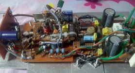
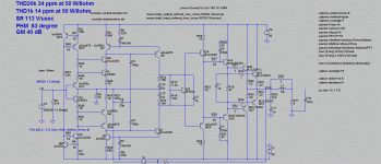
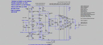
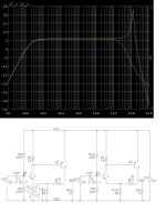
Two CFAs, one with lower distortion (triple OPS) one with higher but with with very musical harmonic distribution (EF2).
Both amps with very good clipping behavior, good PM and GM.
Damir
Both amps with very good clipping behavior, good PM and GM.
Damir
Attachments
Member
Joined 2009
Paid Member
Even the 2nd version has such low THD that I wonder if the distortion profile is relevant ? A musical distortion profile (if accepting the Hiraga style of decreasing harmonics) can be achieved with a relatively simple topology, Singleton input such as the JLH Class AB.
Well given John Broskie's style probably more the latter. Here's a link to the article and basic schematic. I may attempt Mr Wurcer's tests but i scared him off with my last interpretation!
Page Title
Hardly.
The simplest example I can think of, the so called current feedback pair. Making the feedback only the sampled voltage at the emitter of the NPN has dramatic effect on BW and Aol. Even this simple example embodies the major issues. You cannot break the loop properly without the feedback network loading the output as well as appearing in the emitter of the input NPN. The input voltage is impressed across the base of the input device and a resistance to ground, not the base to emitter of the NPN. The current in the feedback network matters hence the simple semantic device to differentiate the two.
Attachments
Well given John Broskie's style probably more the latter. Here's a link to the article and basic schematic. I may attempt Mr Wurcer's tests but i scared him off with my last interpretation!
Page Title
Looks like Peter Walker's phono preamp from circa 1972, updated by Hannes Allmaier in Linear Audio Vol 5.
You guys really should go out more.....😉
Jan
I always thought this was an interesting topology but never built it. It doesn't seem very popular either. I know Hugh has played with it but he never used it. Why has it not been more used - is the current splitting inaccurate ? What if we had a better splitter, something like a transformer perhaps. And throw in a low impedance feedback loop to keep it on topic 🙂
The splitter in the original Blomley circuit consists of two transistors in common base, one NPN and one PNP, tied together at the emitters and driven by a current (that is, from a high-impedance node). The transistors are made of silicon and there is one silicon and one germanium diode setting the difference in base voltages between the NPN and the PNP.
I could imagine that you get a "dead zone" of about 300 mV, if you assume that a silicon diode needs about 600 mV to conduct and a germanium diode about 300 mV (600 mV+600 mV-600 mV-300 mV). As the impedance at the emitter node will always be finite, this could give rise to crossover distortion. Replace the two diodes by a trimmable VBE multiplier and that problem is solved. Or use two pairs of matched transistors, one NPN pair and one PNP pair, and replace the diodes with a diode-connected NPN and a diode-connected PNP.
This correlate my own experiences.Thanks, sharing the same opinion. Just one example of circuit simplicity related to sound quality: as compared many input stages tested in the same amp, whatever changes made to input pair (cascode, tracking cascode, current mirror) or changed it to diamond buffer, it always sounded better with just plain CFA input pair directly connected to rails via collector resistor.
May-be, one day, we will have measurements methods and tools to figure-out 'objectivly' the sound quality of an amplifier. In between, i agree with you: the only way to do the best work and acquire valuable experience is not to look at distortion numbers, or simulation results, but to build in real world, compare and listen. And the best designer is not the one with the most sofisticated measurement instrument, but the one with the best ear and musical culture.
I encourage every designer to follow this track. Of course, audio electronic culture is a requisite, the base of everything. But it is only a first step.
FYI -- as per patents -- I know from personal experience that SIM are allowed in place of measured prototype at the patent office. So, very low THD numbers can be claimed if it was the result from a SIM.
Thx-RNMarsh
Thx-RNMarsh
Two CFAs, one with lower distortion (triple OPS) one with higher but with with very musical harmonic distribution (EF2).
Both amps with very good clipping behavior, good PM and GM.
Damir
I get it.
😎🙂
Thx-RNMarsh
The splitter in the original Blomley circuit consists of two transistors in common base, one NPN and one PNP, tied together at the emitters and driven by a current (that is, from a high-impedance node). The transistors are made of silicon and there is one silicon and one germanium diode setting the difference in base voltages between the NPN and the PNP.
I could imagine that you get a "dead zone" of about 300 mV, if you assume that a silicon diode needs about 600 mV to conduct and a germanium diode about 300 mV (600 mV+600 mV-600 mV-300 mV). As the impedance at the emitter node will always be finite, this could give rise to crossover distortion. Replace the two diodes by a trimmable VBE multiplier and that problem is solved. Or use two pairs of matched transistors, one NPN pair and one PNP pair, and replace the diodes with a diode-connected NPN and a diode-connected PNP.
As far as I remember, the basic drive behind Peter's idea was the same as the drive behind the current dumping idea - produce an amp that needs no adjustment at the production line.
Both idea's succeeded at that goal, but did not produce any better sound quality.
I'm sure that the fact that the concepts were outside mainstream (and thus outside of most designers' knowledge - look at the dozens of article just to explain current dumping) caused them to slowly die a natural dead.
Jan
- Home
- Amplifiers
- Solid State
- CFA Topology Audio Amplifiers