FYI -- as per patents -- I know from personal experience that SIM are allowed in place of measured prototype at the patent office. So, very low THD numbers can be claimed if it was the result from a SIM.
Thx-RNMarsh
AFAIK anything is allowed, including a generator that puts out more than put in. Of course connecting the output to input can't be claimed because that is perpetual motion.🙄 See MEG generators, patents.
I remember, at school, we wrote on each side of a paper "I have discovered the perpetual motion" with 'tsvp' at the bottom, witch means: "Please turn the page".Of course connecting the output to input can't be claimed because that is perpetual motion.
I am more for very low distortion, but this should sound good.
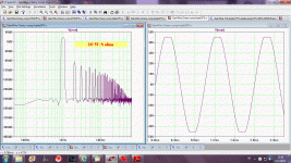
The harmonic distribution for 1W, 10W and 100W.
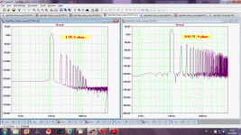
I never built any amp with such high distortion and don't have listening experience with that kind. I am tolking about simulated distortion as I do not have equipment to measure very low distortion.
By the way I expected more CFA schematics here, to learn others configuration, some people keep it secret.
Damir
ps. I use in those CFAs of mine the same front end, it works very well, when I change it for a diamond I've got higher distortion. Use of jfets needs better matching and that is not easy to get.
The harmonic distribution for 1W, 10W and 100W.
I never built any amp with such high distortion and don't have listening experience with that kind. I am tolking about simulated distortion as I do not have equipment to measure very low distortion.
By the way I expected more CFA schematics here, to learn others configuration, some people keep it secret.
Damir
ps. I use in those CFAs of mine the same front end, it works very well, when I change it for a diamond I've got higher distortion. Use of jfets needs better matching and that is not easy to get.
Attachments
Last edited:
Hi Bob,Hi ontoaba,
Just wondering. Do you own a Halcro? Did you AB your amp against a Halcro in the same place and setup? How do you know that your EC had less sonic effect than Halcro's.
No, I don't need to think twice to buy any of such so called hi-end amp or not😉. If you have the reverse job schematic, It may little difference there (dm38 and patent). And to compare just OPS we need to break the amp path.
Halcro VAS is sounded clean and feels clean sound, that some people calling it non memory distortion sound, or wathever they said, but I rather see it is cascoded bjt. The VAS sound is dominant by the feedback, and deep sound is not very bad.
Bruce Candy is good simulator, may be that THD was just sim result that used for marketing, but he moving to class D, and it may turning their advertisements to another story.😕
They selling expensive mining tool too.

Anyway my amp isn't simple😀 It has two type of input stages, two tonal network, one anti oscillating network, one split floating supply, one fatiguing eliminating T path, output passive damper (crossover like but rather a damper), input stages (with opamp), Feedforward path from the opamp to output, and damper manipulating.😱
I really like your amp, looks more like heterodyn receiver or FM transmitter.

If it's so good it definitely deserves proper double sided SMD PCB, what do you think? Can it be published? 😎
I really like your amp, looks more like heterodyn receiver or FM transmitter.
If it's so good it definitely deserves proper double sided SMD PCB, what do you think? Can it be published? 😎
I like your amp too. Yes may be because that inductor with koker so it looks like a transmitter.😀
Yes it is good, but still, some very minor feeling sometimes appeared that may be could still be removed. It is hard to determine what kind of sound it is because very covered by its beauty and not always appeared.
Yes most used EC at RF amplifiying is non feedback (as for LNA is modulating), it will be difficult to implement non feedback in class AB.
.
Maybe not..... it doesn't have to be non-feedback. Just the concepts are interesting and could find application with some small effort. Clever design can bring rewards with cancellation and feedback with CFA.
Thx-RNmarsh
Hardly.
The simplest example I can think of, the so called current feedback pair. Making the feedback only the sampled voltage at the emitter of the NPN has dramatic effect on BW and Aol. Even this simple example embodies the major issues. You cannot break the loop properly without the feedback network loading the output as well as appearing in the emitter of the input NPN. The input voltage is impressed across the base of the input device and a resistance to ground, not the base to emitter of the NPN. The current in the feedback network matters hence the simple semantic device to differentiate the two.
Got it this time. Thank-you.
Clever design can bring rewards with cancellation and feedback with CFA.
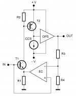
Something like this - combined CFA and VFA with EC, positive features from both worlds.

Attachments
An EC is normally local, so it will help the slow of main feedback.
Something like this - combined CFA and VFA with EC, positive features from both worlds.
LT1166
Hi Marcel,
First, thank you for your reply.
As for the LT1166, indeed, they do have a communication problem. LT told me that the guy who designed the LT1166, has left the company soon after it was released. For this reason they were unable to explain some discrepancies between the description in the datasheet and the real properties of this IC. I bet you are not the only one who is misled by the datasheet. The discrepancies that I have discovered became apparent after fiddling with a SPICE model at the device level (courtesy of Ovidiu Popa), which revealed the real behavior of this chip.
Regarding distortion of a sliding bias circuit, things are more complicated, as opposing mechanisms are involved. On the one hand, as you argued, it's beneficial to not completely switch off the O/P devices, as it eases the turn on. On the other hand, fixing the minimum O/P device current to say 1/2 Iq, will increase the modulation of the bias voltage*, which in turn will introduce more distortion. Right now I'm not sure which of two mechanisms will 'win' and it needs further experimental investigations.
*Please have a look at this post.
>Dutch quote
I like it too (of course). It is so beautifully worded.
Cheers,
Edmond.
Hi Edmond,
I never actually used the LT1166, my comments are based on the information I read about it when it was introduced. If Linear Technology implemented a harmonic mean rule or something similar in the LT1166 but state in its data sheet that they used a product rule, then what I've written is clearly not valid (and Linear Technology then obviously has an internal communication problem).
Hi Marcel,
First, thank you for your reply.
As for the LT1166, indeed, they do have a communication problem. LT told me that the guy who designed the LT1166, has left the company soon after it was released. For this reason they were unable to explain some discrepancies between the description in the datasheet and the real properties of this IC. I bet you are not the only one who is misled by the datasheet. The discrepancies that I have discovered became apparent after fiddling with a SPICE model at the device level (courtesy of Ovidiu Popa), which revealed the real behavior of this chip.
I fully agree with you that the inactive device should not switched off entirely or almost entirely, though mainly for another reason. In case of a constant product (geometric mean) rule, the minimum current of the inactive device will reach a problematic low level, only a few milliamps. Across a typical RE of 0.22 Ohm, this means a voltage drop of 1mV or less. If the offset voltage of the sensing circuitry is larger than this (that is, in the 'wrong' direction) it will wreak havoc, as it tries (in vain!) to create a negative voltage across RE, which is impossible. As a result, the bias voltage will rise to a totally inappropriate high level and causing lots of distortion. This situation should be avoided at any cost.In the literature you see that many authors prefer non-switching output stages, that is, output stages where the current through one output device approaches some nonzero value (like half the quiescent current) when the current through the other gets large. The supposed advantage is that the inactive device can turn on quickly when it is already biased at a reasonable current rather than switched off entirely or almost entirely. This behaviour is easy to achieve with a class AB control loop by choosing a control rule that lets the current through one device approach some nonzero minimum value when the current through the other output device tends to infinity.
I don't know what effect this has on the distortion measured with sine waves or with actual music, I never compared the distortion of otherwise similar amplifiers with exp(-I1*R)+exp(-I2*R), harmonic mean and product control rules.
By the way, I like the fact that you put a Dutch quote below your posts.
Best regards,
Marcel
Regarding distortion of a sliding bias circuit, things are more complicated, as opposing mechanisms are involved. On the one hand, as you argued, it's beneficial to not completely switch off the O/P devices, as it eases the turn on. On the other hand, fixing the minimum O/P device current to say 1/2 Iq, will increase the modulation of the bias voltage*, which in turn will introduce more distortion. Right now I'm not sure which of two mechanisms will 'win' and it needs further experimental investigations.
*Please have a look at this post.
>Dutch quote
I like it too (of course). It is so beautifully worded.
Cheers,
Edmond.
Not found fast enough ICs for EC 0° phase at HF.Something like this - combined CFA and VFA with EC, positive features from both worlds.
*Please have a look at this post.
Also follow the discussion around that thread, regarding "gm doubling". Edmond's conclusion about the bias voltage modulation is physically incorrect. In terms of causality, it's the gm modulation (worst case, doubling) that is at the root of the "crossover distortions".
Feedback based non-switching bias schemes have the same underlying mechanism: the available loop gain linearizes the output stage transconductance.
Hi Marcel,
I fully agree with you that the inactive device should not switched off entirely or almost entirely, though mainly for another reason. In case of a constant product (geometric mean) rule, the minimum current of the inactive device will reach a problematic low level, only a few milliamps. Across a typical RE of 0.22 Ohm, this means a voltage drop of 1mV or less. If the offset voltage of the sensing circuitry is larger than this (that is, in the 'wrong' direction) it will wreak havoc, as it tries (in vain!) to create a negative voltage across RE, which is impossible. As a result, the bias voltage will rise to a totally inappropriate high level and causing lots of distortion. This situation should be avoided at any cost.
Cheers,
Edmond.
Hi Edmond,
I looked at the innards of the LT1166 SPICE model several years ago. I don't remember the details, but I'm pretty sure it is fairly well-behaved and does not have a tendency like you described even when there are slight Vbe mismatches. It is a fairly clever translinear circuit.
Cheers,
Bob
Something like this - combined CFA and VFA with EC, positive features from both worlds.
And, when you combine the whole thingy into symmetrical, complimentary, push-pull... etc what do you get for a schematic?
Thx-RNMarsh
Not found fast enough ICs for EC 0° phase at HF.
Yes clearly, but in this case in discrete way and just as an error correction signal added to the regular CFB.
Attachments
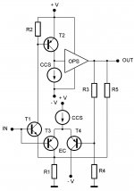
Yes clearly, but in this case in discrete way and just as an error correction signal added to the regular CFB.
Umm,.. isn't that just half CFA? Is that combination better than separated?
Last edited:
We could say CFA supported by VFA. Better, well just an idea, performance should be simmed and measured in practice.
I tried-it. Too tricky for mass production on my point of view as we just reduce the phase margin (for the same reason). I don't want to report my listening experience of those tries to not influence you, if you try-it in future. One objective point is you get better distortion numbers and speaker's damping.Yes clearly, but in this case in discrete way and just as an error correction signal added to the regular CFB.
- Home
- Amplifiers
- Solid State
- CFA Topology Audio Amplifiers