
Hi all.
I remember reading somewhere on this forum, that the resistors on the current mirror should be at least twice the value of the ltp degeneration resistors.
Unfortunatly I don't remember the reason for this. Looking at your latest schematic, your values are the opposite of that, with 47 ohms on the current
mirror and 100 ohms on the ltp. Can someone please elaborate on this?
Keep going lineup
Well done. unfortunately I am a bit lazy with my explanations🙄#259 Ultima Thule
#189 bucks bunny
#190 wahab
I am sorry that their advice and arguments are not understood at all.
This worst case scenario is
When the output is saturated at the negative rail, the current flowing through U6 is zero, so U7 becomes just a base-emitter diode.
Therefore, R3 + its diode steals most of the current flowing to the reference voltage D3 + D2.
As a result, the reference voltage drops, and the current flowing through the IPS also sharply decreases.
When IPS turns off, all positive side transistors U3, U4, U11, U10, and U11 also turn off, causing latch-up with the output stuck to the negative side.
Lineup, your latest schematics seem to approximate the worst case scenario.
brian,
Rather than relying on the results of spice or the circuits of famous designers, we recommend that you get into the habit of thinking about ``why things are the way they are.''
If you do that, I think you'll come up with the idea, ``Let's check the U5 current to see what happens to the IPS tail current when the output clips.''
In this way, simulation will become a more useful tool.
View attachment 1246271
View attachment 1246273
Furthermore, "U7 should generate heat, so what will happen if that happens?"
When Q7 is 75℃
(The dotted line is the original room temperature value)
View attachment 1246288
(The dotted line is the original room temperature value)
Fortunately I never became a teacher
Furthermore, "U7 should generate heat, so what will happen if that happens?"
Very good, this is the stuff that the sim doesn't show! @peufeu wrote a lot about it in his "memory distortion" series.
I'd like to compare cascode versus non-cascode like he did for LTP, VAS, CCSs. Haven't gotten around to it.
(BTW, I think the next level in simulation would be exactly this: modelling the instantaneous junction temperature and its effects. Does such a simulator exist?)
I believe I mentioned earlier that U6 and U7 will likely benefit from heatsinks. Shouldn't take much though.
,

I cascoded LTP, VAS and CCS in sims and the difference was such that I'll apply it. VAS now provides over 80 dB of gain, LTP, 100 dB. However the sims regard (closely) matched pairs, probably unobtainium by now. With compensation disabled, gain plot isVery good, this is the stuff that the sim doesn't show! @peufeu wrote a lot about it in his "memory distortion" series.
I'd like to compare cascode versus non-cascode like he did for LTP, VAS, CCSs. Haven't gotten around to it.
(BTW, I think the next level in simulation would be exactly this: modelling the instantaneous junction temperature and its effects. Does such a simulator exist?)
Blameless has 100 degeneration and 68 Ohm current mirror.Hi all.
I remember reading somewhere on this forum, that the resistors on the current mirror should be at least twice the value of the ltp degeneration resistors.
Unfortunatly I don't remember the reason for this. Looking at your latest schematic, your values are the opposite of that, with 47 ohms on the current
mirror and 100 ohms on the ltp. Can someone please elaborate on this?
Keep going lineup
I now have 100 degeneration and 52 Ohm current mirror.
Current mirror is 47 Ohm + 5 Ohm from the DC-offset potentiometer.
Hi all.
I remember reading somewhere on this forum, that the resistors on the current mirror should be at least twice the value of the ltp degeneration resistors.
Unfortunatly I don't remember the reason for this. Looking at your latest schematic, your values are the opposite of that, with 47 ohms on the current
mirror and 100 ohms on the ltp. Can someone please elaborate on this?
Keep going lineup
I think it's about noise.
The theory of low-noise design is to reduce the noise generated in the first stage and increase the gain of the first stage as much as possible so that the noise generated in the second stage can be ignored. Although you may not think of the current mirror as a second stage, it still generates noise. The current mirror's degenerate resistor generates first stage noise that is proportional to the value of the resistor, but the thermal noise generated from the degenerate resistor is proportional to the square root of that value.
In other words, by lowering the LTP degeneration resistance and increasing the mirror degeneration resistance, the first stage noise can overwhelm the thermal noise generated by the mirror degeneration resistance.
(Note that even if the noise in the first stage increases, the signal component also increases, so the S/N does not change.)
Of course, we also have to consider the noise generated by transistors, but here I am only considering resistors to keep things simple.
However, in the case of a power amplifier, it is not so severe, and if you are concerned about it, you will have to lower the values of R8 and R21 in circuit diagram #269 before that, so I am not concerned about this.
By the way, It seems strange that increasing the resistor reduces noise, so much so that even professional designers sometimes fail to notice.
When TL08x was first released, this resistance was 610Ω and the noise was 25nV/√Hz. Later, he realized that increasing this resistance would reduce noise, and changed it to 1080Ω and released it as TL07x (18nV/√Hz). After a while, the TL08x was also changed and now both are 18nV/√Hz.
You can see that noise increases when a low value trim pot is attached to the offset adjustment terminal.
P.S. Oh, and it also happens to be an answer to the lineup.
Attachments
Last edited:
I tested setting LTP degen to 33+33 Ohm.
This really changed the amplifier. More gain and more TMC compensation was the result.
I now stick to 100+100 Ohm in LTP.
And increased mirror resistor to 68+68 Ohm. (Making them 73+73 Ohm including the offset adjust)
This gives lower compensation and lower distortion overall.
This really changed the amplifier. More gain and more TMC compensation was the result.
I now stick to 100+100 Ohm in LTP.
And increased mirror resistor to 68+68 Ohm. (Making them 73+73 Ohm including the offset adjust)
This gives lower compensation and lower distortion overall.
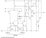
Here is the current schematic.
I have lowered the gain of the amplifier. Making R8 1.8k.
Changed mirror resistors to 68 Ohm.
Increased the VAS emitter resistor to 18 Ohm.
Changed TMC compensation.

I have lowered the gain of the amplifier. Making R8 1.8k.
Changed mirror resistors to 68 Ohm.
Increased the VAS emitter resistor to 18 Ohm.
Changed TMC compensation.
'Final' schematic.
Has very low distortion. THD 0.000045%
Changes:
Setting mirror emitter resistors to 56 Ohm.
Removed VAS transistor emitter resistor = U6
Adjusted TMC compensation for lowest possible distortion.

Has very low distortion. THD 0.000045%
Changes:
Setting mirror emitter resistors to 56 Ohm.
Removed VAS transistor emitter resistor = U6
Adjusted TMC compensation for lowest possible distortion.
Reflecting characteristic changes due to instantaneous temperature changes It seems that a Virtual Bipolar Inter-Company model has already been developed, but I am not familiar with it at all. I think there is spice software that supports that model, but it's probably not free.(BTW, I think the next level in simulation would be exactly this: modelling the instantaneous junction temperature and its effects. Does such a simulator exist?)
The noise of emitter degeneration resistors clearly shows up in my sims (µ-cap enables plot of THD+N) to the extent that one wants to eliminate it. In noninverting designs, the R of the input filter is a major noise source as well. One way to reduce it is to apply more NFB (decreasing overall AC gain). That in turn increases the (undesirable) "varactor" effect. Hence an inverting amp might be the better alternative as it minimizes the AC involved over the LTP. BTW for the LTP, duals still are available (with better specs than the ones I intend to use).I think it's about noise.
The theory of low-noise design is to reduce the noise generated in the first stage and increase the gain of the first stage as much as possible so that the noise generated in the second stage can be ignored. Although you may not think of the current mirror as a second stage, it still generates noise. The current mirror's degenerate resistor generates first stage noise that is proportional to the value of the resistor, but the thermal noise generated from the degenerate resistor is proportional to the square root of that value.
In other words, by lowering the LTP degeneration resistance and increasing the mirror degeneration resistance, the first stage noise can overwhelm the thermal noise generated by the mirror degeneration resistance.
(Note that even if the noise in the first stage increases, the signal component also increases, so the S/N does not change.)
Of course, we also have to consider the noise generated by transistors, but here I am only considering resistors to keep things simple.
However, in the case of a power amplifier, it is not so severe, and if you are concerned about it, you will have to lower the values of R8 and R21 in circuit diagram #269 before that, so I am not concerned about this.
By the way, It seems strange that increasing the resistor reduces noise, so much so that even professional designers sometimes fail to notice.
When TL08x was first released, this resistance was 610Ω and the noise was 25nV/√Hz. Later, he realized that increasing this resistance would reduce noise, and changed it to 1080Ω and released it as TL07x (18nV/√Hz). After a while, the TL08x was also changed and now both are 18nV/√Hz.
You can see that noise increases when a low value trim pot is attached to the offset adjustment terminal.
P.S. Oh, and it also happens to be an answer to the lineup.
https://www.mouser.com/datasheet/2/609/SSM2212-3131582.pdf
The Baker Clamp diode works well.
It limits the output and produces an almost symmerical Clipping.

It limits the output and produces an almost symmerical Clipping.
It is a good idea.The noise of emitter degeneration resistors clearly shows up in my sims (µ-cap enables plot of THD+N) to the extent that one wants to eliminate it. In noninverting designs, the R of the input filter is a major noise source as well. One way to reduce it is to apply more NFB (decreasing overall AC gain). That in turn increases the (undesirable) "varactor" effect. Hence an inverting amp might be the better alternative as it minimizes the AC involved over the LTP. BTW for the LTP, duals still are available (with better specs than the ones I intend to use).
https://www.mouser.com/datasheet/2/609/SSM2212-3131582.pdf
To add dual matched transistors.
Mouser has 14000 in stock: https://www.mouser.se/ProductDetail/Analog-Devices/SSM2212RZ-R7?qs=WIvQP4zGang/JsE6b4gfRA==
Two remarks:
Ideally you want the bases of the differential to see the same impedance.
Afaik only electrostatic speakers need that large of an inductor for stability. Most builders will be happier with a small inductor.
Ideally you want the bases of the differential to see the same impedance.
Afaik only electrostatic speakers need that large of an inductor for stability. Most builders will be happier with a small inductor.
@Alexandre
Inductor 6uH was chosen because of Rod Elliott
https://sound-au.com/amp_design.htm#s34
Bases see same impedance. Yes.
Haven't I already same impedances?
Any changes so suggest?
Inductor 6uH was chosen because of Rod Elliott
https://sound-au.com/amp_design.htm#s34
Bases see same impedance. Yes.
Haven't I already same impedances?
Any changes so suggest?
The bases see the parallel of those resistances AND you have to consider all the caps and potentiometer as well. Now you see why I used the word impedance?
Here is the thing. I don't know how much of a difference it makes in practice, I have not compared every possible way of building an amplifier. But it makes a difference, even in the simulator (if you know how to "ask"). Being the perfectionist that I am, I would go for something like this, OR, the equivalent of it in inverting mode.

Here is the thing. I don't know how much of a difference it makes in practice, I have not compared every possible way of building an amplifier. But it makes a difference, even in the simulator (if you know how to "ask"). Being the perfectionist that I am, I would go for something like this, OR, the equivalent of it in inverting mode.
- Home
- Amplifiers
- Solid State
- Cello One. Good Amplifier 15 Watt with TMC and Laterals