Hi Mark,
That isn't a diamond buffer. Your design is off-topic for this thread, just saying.
-Chris
That isn't a diamond buffer. Your design is off-topic for this thread, just saying.
-Chris
Bob Cordell's output stage is a conventional MOSFET complementary source follower, not shown here. However his approach to eliminating clipping artifacts (see post #97) is applied to the front end of the amplifier, and can be used with most power amp designs, including the one shown in post #98.
Cordell's concept works well; I exhibited my implementation recovering from clipping (btw no MOSFETs), because Cordell's paper contains no scope photos of clipping. I've simply offered simulation evidence that the idea achieves its objective: graceful clipping and clipping recovery.
Cordell's concept works well; I exhibited my implementation recovering from clipping (btw no MOSFETs), because Cordell's paper contains no scope photos of clipping. I've simply offered simulation evidence that the idea achieves its objective: graceful clipping and clipping recovery.
This description fundamentally changes the intent of your post. I wasn't aware that you were trying to be helpful with the front end changes instead of showing your version of an over the top amplifier design which did not show any similarities to a diamond configuration. Your circuit would require modification to operate with a diamond output stage, like shorting D8 for starters, which eliminates a pile of components. Otherwise, yeah. I can see you can drive a diamond buffer output stage with it. Same for almost any other voltage amplification stage.
-Chris
-Chris
Bob Cordell's output stage is a conventional MOSFET complementary source follower, not shown here. However his approach to eliminating clipping artifacts (see post #97) is applied to the front end of the amplifier, and can be used with most power amp designs, including the one shown in post #98.
Cordell's concept works well; I exhibited my implementation recovering from clipping (btw no MOSFETs), because Cordell's paper contains no scope photos of clipping. I've simply offered simulation evidence that the idea achieves its objective: graceful clipping and clipping recovery.
It would be nice if you explain in a few sentences how your suggestion works, since you
do not show a schematic or simulation file. Why don't you since everything in this thread
has been in the open?
How close to the rails will your amp go with the clamping in place?
The vast majority of clipping misbehaviors arise in the front end, so that's the place to fix em. Cordell's textbook offers a half dozen different fixer upper subcircuits, some of them very cute, to tame misbehavior. However the clamp ideas which appeal to me, personally, are the ones from waaaay back in his 1982 paper.
Any signal node with a high impedance load (current source or current mirror), can potentially misbehave during clipping. A tiny amount of input overdrive can produce a gigantic output swing. So these are the places to investigate first.
Any signal node with a high impedance load (current source or current mirror), can potentially misbehave during clipping. A tiny amount of input overdrive can produce a gigantic output swing. So these are the places to investigate first.
Thanks for that! Indeed it is awfully similar. Shows there's nothing new in electronics.
I'm a huge fan of Lee. I reckon most things I know about RFIC design are straight out of his book "The design of CMOS RFICs". The book is worth buying for the "non-linear history of radio" chapter alone.
Looks to me as if the bottom of R16 (resistor below Q6 should go to R17 and not R15, in
the Harris 2539 (page 23), anyone agree?
https://web.stanford.edu/class/archive/ee/ee214/ee214.1042/Handouts/ho15opamp.pdf
Pete, Bob Cordell explains the clamp circuits in his paper. It's in section 2.1 on the eighth page of the .pdf, specifically in paragraphs 3 and 7. Scan for the phrases "D2 and D3" , and also "D4-D7".
(Here is a link) . Bob presented the paper at the AES Convention in October 1982, but they didn't get around to publishing it in their hardcopy Journal, until January 1984.
_
(Here is a link) . Bob presented the paper at the AES Convention in October 1982, but they didn't get around to publishing it in their hardcopy Journal, until January 1984.
_
Last edited:
The vast majority of clipping misbehaviors arise in the front end, so that's the place to fix em. Cordell's textbook offers a half dozen different fixer upper subcircuits, some of them very cute, to tame misbehavior. However the clamp ideas which appeal to me, personally, are the ones from waaaay back in his 1982 paper.
Any signal node with a high impedance load (current source or current mirror), can potentially misbehave during clipping. A tiny amount of input overdrive can produce a gigantic output swing. So these are the places to investigate first.
Cross conduction usually happens in the output stage unless you do not drive them
deep into saturation.
Pete, Bob Cordell explains the clamp circuits in his paper. It's in section 2.1 on the eighth page of the .pdf, specifically in paragraphs 3 and 7. Scan for the phrases "D2 and D3" , and also "D4-D7".
(Here is a link) . Bob presented the paper at the AES Convention in October 1992, but they didn't get around to publishing it in their hardcopy Journal, until January 1984.
Thanks, yes I am familiar with that paper and will take another look at those sections.
The vast majority of clipping misbehaviors arise in the front end, so that's the place to fix em. Cordell's textbook offers a half dozen different fixer upper subcircuits, some of them very cute, to tame misbehavior. However the clamp ideas which appeal to me, personally, are the ones from waaaay back in his 1982 paper.
Any signal node with a high impedance load (current source or current mirror), can potentially misbehave during clipping. A tiny amount of input overdrive can produce a gigantic output swing. So these are the places to investigate first.
IME the clipping misbehavior in the front end happens because the output stage has hit
the rail and therefore all the feedback gain causes the front end and drivers to "try"
at full current to fix the situation. Similarly, when the output stage sticks the feedback
and front end "try" with all the available current to get it out of the stuck condition. The
current spikes are often very large.
I never really dug into Cordell's clamping methods, I'll have to spend some time on them.
The datasheet could be wrong. I see that it does agree with Lee's writeup.
Liking the ideas here
I recently made a small pp amplifier using a pair of TIP41/42 in a simple diode biased stage very similar to this. This stage is within the fb loop of a parts bin opamp...LF353.
Humble parts and design but surprisingly satisfying!
Unfortunately I have no good way of measuring THD at 1kHz. But at least at 100Hz THD and N was below 0.5% up to just over 4 watts into 8 ohms. It makes a neat headamp.
Mark, the Cordell clipping desticker circuit is awesome! Thankyou so much for pointing me to that - it improves the behaviour of my amp no end.
Totally not OT - very useful bit of info.
I put the clipping desticker circuit after the VAS stage, controlling the VAS transistor bases and collectors. I found the diode capacitance at the base of the VAS transistor messed with my compensation and killed the THD as a result, so I threw some series resistors in to prevent that. It doesn't prevent the clipping desticker from working as it should, but does stop it loading up the VAS bases unnecessarily.
Again, thanks!
Attachments
I (and also Bob Cordell) use 1N4149 diodes for the clampsters. Datasheet guarantees half the capacitance of a 1N4148. And since you are OK with SMD devices, you could select the Toshiba 1SS472L3 diodes instead. These little jewels have 13X lower capacitance than 1N4148. Boy howdy.
Toshiba 1SS472L3 diodes
That was a difficult one to find, some of the closest I found from Toshiba was BAS316, any web link to your super diode?
Diodes | Products | TOSHIBA Semiconductor & Storage Products | Asia-Pacific
EDIT: Typo, I think I found it!
1SS427 | Switching Diodes | TOSHIBA Semiconductor & Storage Products | Asia-Pacifichttps://toshiba.semicon-storage.com/info/lookup 1SS427
Last edited:
Im following this with interest as it seems like a good companion for my Tabaq fullrange speakers. Im seriously thinking about building one active version, and this amp may be the solution.
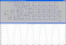
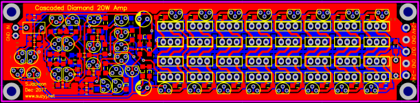
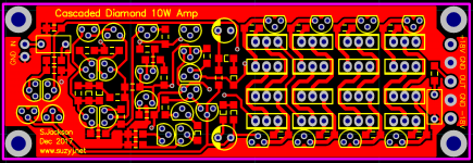
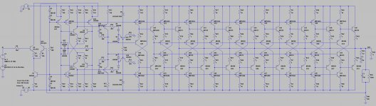
New layout with clipping management incorporated. I moved the output drivers to the side rather than the top - it makes it a lot easier to generate different versions by simply adding or removing blocks on the output. Size for 2, 4, and 8 sets of output diamonds is 1.25" wide by 3", 3.75" and 5.25" respectively, so despite the large number of transistors the boards are small.
The 8-set version (20W into 8 ohms, 40W into 4 ohms) has to run at +/-24 rather than +/-18, meaning the 2N3904/3906 are no longer suitable for VAS duty and other full-rail jobs. The MPSA06 & MPSA56 are an acceptable substitute here - they do 80V, 0.5A, 625mW, and aren't that much slower. As a bonus they have the same pinout as the 2N parts, unlike BC5XX transistors. THD for 40W into 4 ohms for the MPSA version is ~5ppm.
The 8-set version (20W into 8 ohms, 40W into 4 ohms) has to run at +/-24 rather than +/-18, meaning the 2N3904/3906 are no longer suitable for VAS duty and other full-rail jobs. The MPSA06 & MPSA56 are an acceptable substitute here - they do 80V, 0.5A, 625mW, and aren't that much slower. As a bonus they have the same pinout as the 2N parts, unlike BC5XX transistors. THD for 40W into 4 ohms for the MPSA version is ~5ppm.
Attachments
-
 Screen Shot 2017-12-21 at 3.56.25 pm.png685.1 KB · Views: 485
 -
 Screen Shot 2017-12-21 at 3.55.44 pm.png592.7 KB · Views: 464
 -
 Screen Shot 2017-12-21 at 3.55.05 pm.png474.1 KB · Views: 463
 -
 Screen Shot 2017-12-21 at 4.03.50 pm.jpg637.8 KB · Views: 453
 -
40W BD179 Amp with diamond output and npn input - clipping management.asc24 KB · Views: 160
- Home
- Amplifiers
- Solid State
- Cascading diamond buffers - a cheap low THD 10W amp with TIP41C