How the I/V stage presented in post #9243 can be used in this differential version? is it sufficient to simply remove the phase splitter and duplicate the ciricuit?
Pretty much so. Double up. Bias circuitry can and should be shared.
On the buffer take the upper resistor and output away, connect directly to +V. Or change the buffer to whatever style you like.
Thor

Haizzz ChatGPT is new Gen doesn't know anything about great vintage Dac's Iggy. LolIt is progressing everyday, don't focus on what I posted above.
And changes migth happen with Thorsten Losch ideas and Icsaszar work.
I tried to ask CHATGPT about op amps or what the best dac and I was disapointed by the answers and I almost was out to learn bag pipes because of it!
Seems it diosn't know about New ones too and it doesn't find my keys when I forget where they are.
Maybe I ask the wrong questions ?!
"Please ChatGPT, what the difference between a red Cerafin and a Black Gate ? " 🤔😎
Maybe I ask the wrong questions ?!
"Please ChatGPT, what the difference between a red Cerafin and a Black Gate ? " 🤔😎
In my experience it is very good for specific applications.ChatGPT? Artificial, yes. Intelligence? About 1/100 of Googles algorithm.
For example with mic input I ask 'what is the dollar amount saved per month if I switch from x.xx% to x.xx% interest rate', loan amount is $(x) and taken over (x.xx) years, periodicity of payments is (x). It shows the arithmetic and performs the calcs. You can follow up directly and amend any of the variables and ask it to recalc.
If you asked it 'how to' PCB for 1541A .. google is probably better ..
Cheers to all 🙂
Last edited:
Hahha.. ask it for lowest THD output stage - build that, and then run for the hills (with hands over ears).It is progressing everyday, don't focus on what I posted above.
And changes migth happen with Thorsten Losch ideas and Icsaszar work.
I tried to ask CHATGPT about op amps or what the best dac and I was disapointed by the answers and I almost was out to learn bag pipes because of it!
It's true, I thought just the same thing a few days ago... 😉you guys are awesome ..
Sediment aside, agree 100% with Bali Kopi - bolehkah saya minta susu dengan ini?-----
Balinese ordinary coffee is phenomenal, just little short of famous Kopi Luwak.
Further 'out the **** of a jungle cat brew' - I also liked it very much ..
I also tried the jungle cat (for real) - Kumpung Dujoh, Sarawak (near to Bau)
Last edited:
Surikin border (Malaysia/Indo)
Selling full-comb honey in 20L (mayo) buckets, bees for free, skulls at the bridge - much the same.
Tsing Tao boxes, same price (generally speaking) cheapest (good) beer in the world - 5 for 5 on ice in Kuching.
Good night 🙂
Selling full-comb honey in 20L (mayo) buckets, bees for free, skulls at the bridge - much the same.
Tsing Tao boxes, same price (generally speaking) cheapest (good) beer in the world - 5 for 5 on ice in Kuching.
Good night 🙂
Ideas needed for better understanding the DEM filter circuit
What is the impedance of the DEM filter pins where the external capacitors are connected? Do the capacitors need to be the same, or different? If some pins are lower impedance, the capacitor attached there should be higher capacitance, for achieving the same ripple rejection - so I think.
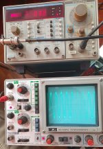
I can generate special I2S signal where each bit 9 to 15 can be turned on individually. All other bits remain zero, except the bit being turned on. This results in an analog DC output between ~0 mA and -2 mA (~0 V to +3 V after I/V conversion). Then I inject a 440 Hz current "disturbance" into the selected DEM pin and observe the analog output. I injected 1 Vrms via a 10M resistor and a DC blocking capacitor. Here is what I get:
Bit 9: 27 uVrms
Bit 10: 54 uVrms
Bit 11: 99 uVrms
Bit 12: 71.4 uVrms
Bit 13: 97.5 uVrms
Bit 14: 97.7 uVrms
Bit15: 128 uVrms
All other bits show just DC and some noise, except the bit being "disturbed".
The impedance of the DEM pins is clearly not the same, because they attenuate the input signal of fixed 10M source impedance differently.
I am stuck at the intepretation.
What is the impedance of the DEM filter pins where the external capacitors are connected? Do the capacitors need to be the same, or different? If some pins are lower impedance, the capacitor attached there should be higher capacitance, for achieving the same ripple rejection - so I think.
I can generate special I2S signal where each bit 9 to 15 can be turned on individually. All other bits remain zero, except the bit being turned on. This results in an analog DC output between ~0 mA and -2 mA (~0 V to +3 V after I/V conversion). Then I inject a 440 Hz current "disturbance" into the selected DEM pin and observe the analog output. I injected 1 Vrms via a 10M resistor and a DC blocking capacitor. Here is what I get:
Bit 9: 27 uVrms
Bit 10: 54 uVrms
Bit 11: 99 uVrms
Bit 12: 71.4 uVrms
Bit 13: 97.5 uVrms
Bit 14: 97.7 uVrms
Bit15: 128 uVrms
All other bits show just DC and some noise, except the bit being "disturbed".
The impedance of the DEM pins is clearly not the same, because they attenuate the input signal of fixed 10M source impedance differently.
I am stuck at the intepretation.
John from ECDESIGNS here, talked a lot about the importance of the inductance in the 14 DEM layout decoupling ( to a point he said they could be also layouted vertically // to the TDA DEM pins with top head soldered directly on the pins near the body of the TDA, with other side with the AGnd around the pcb pin pad !
Certainly overkill and too much hardcore DIY. I don't remember however he talked about the capacitance of the caps according the MSB/LSB... If I am rigth, P. Rogic is more about 0.1 uF on each with the circa close 200 K Hz frequency made with the passive free DEM 470 pF advised by Philips. IIRC he inputed on Audial blog or a paper it was not crucial to be noticeable enough by ears related to the rest around the TDA1541A (front end, PS, I/V... chip origin...)
Could be interresting to test if beyond the better measurement here according the capacitances chhoice pin to pin, a listening test can weither or not check a difference. It's like some THD measurements, to a point, it is eyes reassurement more than anything else.
Looking forward to read your results.
Last edited:
Waaaa bahasa indonesia boleh juga ya mantap. KudosSediment aside, agree 100% with Bali Kopi - bolehkah saya minta susu dengan ini?
Further 'out the **** of a jungle cat brew' - I also liked it very much ..
I also tried the jungle cat (for real) - Kumpung Dujoh, Sarawak (near to Bau)
For example with mic input I ask 'what is the dollar amount saved per month if I switch from x.xx% to x.xx% interest rate', loan amount is $(x) and taken over (x.xx) years, periodicity of payments is (x). It shows the arithmetic and performs the calcs. You can follow up directly and amend any of the variables and ask it to recalc.
Google sends me here:
https://www.savings.com.au/calculators/home-loan-calculator
Ideas needed for better understanding the DEM filter circuit
What is the impedance of the DEM filter pins where the external capacitors are connected? Do the capacitors need to be the same, or different? If some pins are lower impedance, the capacitor attached there should be higher capacitance, for achieving the same ripple rejection - so I think.
I can generate special I2S signal where each bit 9 to 15 can be turned on individually. All other bits remain zero, except the bit being turned on. This results in an analog DC output between ~0 mA and -2 mA (~0 V to +3 V after I/V conversion). Then I inject a 440 Hz current "disturbance" into the selected DEM pin and observe the analog output. I injected 1 Vrms via a 10M resistor and a DC blocking capacitor. Here is what I get:
Bit 9: 27 uVrms
Bit 10: 54 uVrms
Bit 11: 99 uVrms
Bit 12: 71.4 uVrms
Bit 13: 97.5 uVrms
Bit 14: 97.7 uVrms
Bit15: 128 uVrms
All other bits show just DC and some noise, except the bit being "disturbed".
The impedance of the DEM pins is clearly not the same, because they attenuate the input signal of fixed 10M source impedance differently.
Absolutely not. You inject into a pin with or without filter capacitor?
Did you look at the various published internal schematics and it becomes clearer.
Each DEM Filter pin looks into a cascode emitter via a resistor. Resistor values vary with current. The collector of this cascode is cascoded again with a second cascode...
So the input impedance and RC time consonant on the filter vary with pin.
Thor
To enlarge, each pin receives a divided and splitter current, which starts out as 4mA.So the input impedance and RC time consonant on the filter vary with pin.
Each division is 1x n uA -> 4 x n/4 uA.
The first division is 4mA -> 4 x 1mA.
The worst case error for each of the 4 currents is +/-5%. So we cannot use this for a precision DAC.
The genius of RJvdP was to add 16 switches to these 4 currents.
This each of the 4 currents with up to +/- 5% error can be switched to each of the 4 outputs and the DEM logic does exactly that.
Over 4 periods of the DEM Clock, each output has all 4 currents injected into it, for 1/4 of the time. So now over a period of 4 DEM clock the average error becomes zero.
The MSB current of each divider uses 2 currents, the lower bit gets 1 current, the remaining current is divided again.
So the MSB pin gets a current of 2 x 1mA at a frequency of 1/2 DEM for the ripple caused by the 5% error of the individual currents. If we presume similar voltage drop across the filter resistor, this pin will have the lowest input impedance. I believe it's around 1k (so with 100n it's a 100uS time constant and a 1.6kHz turnover, which will kill any ripple at 88kHz by 34dB. Going to 1uF attenuates ripple here by 54dB.
The next pin gets a current of 1 x 1mA at a frequency of 1/4 DEM for the ripple caused by the 5% error of the individual currents. So in theory we can expect the resistor value to double.
The next pin is actually the MSB of the next divider which gives 4 X 0.25mA. so the third pin gets a current of 2 x 0.25mA at a frequency of 1/2 DEM for the ripple caused by the 5% error of the individual currents. So in theory we can expect the resistor value to be 4 times that of the MSB pin.
The next pin gets a current of 1 x 0.25mA at a frequency of 1/4 DEM for the ripple caused by the 5% error of the individual currents. So in theory we can expect the resistor value to be 8 times that of the MSB pin.
The next pin is actually the MSB of the third divider which gives 4 X 62.5uA. so the fifth pin gets a current of 2 x 62.5uA at a frequency of 1/2 DEM for the ripple caused by the 5% error of the individual currents. So in theory we can expect the resistor value to be 16 times that of the MSB pin.
The next pin gets a current of 1 x 62.5uA at a frequency of 1/4 DEM for the ripple caused by the 5% error of the individual currents. So in theory we can expect the resistor value to be 32 times that of the MSB pin.
The final pin is again 1 X 62.5uA and likely the same resistor value. It's output drives the multiemitter current divider that divides up the remaining currents.
The first divider uses 512 transistors in parallel, each transistor can have 5% error, each time we double the number of transistors, the error reduces by sqrt👎, so worst case error on bit 7 is 0.22%
Another 511 transistors form the rest of the divider, 256 for the next bit and so on.
That is how each bit current is generated.
The input impedance of each DEM pin could be measured directly using an AC impedance meter. Or set the IC to digital silence and inject a current of (say) 1/10th of the nominal pin current and measure the resultant voltage, V/I = Z.
Thor
You inject into a pin with or without filter capacitor?
With 100 nF filter capacitors. Xc = 3.6k @ 440 Hz.
If the pin impedance is higher, the attenuated voltage on the capacitor is lower at this frequency. From this we can conclude the ratio of the internal impedance of each DEM pin. Bit 9 is highest, bit 15 is lowest. And the capacitances should be reciprocal to get the same time constant (-> attenuation of DEM oscillator ripple), if all this is true.
That is about 1-2-4-3-4-4-5 capacitance ratios for bit 9 to bit 15.
I don't understand bit 12, and I am not sure if my conclusion is correct.
I will measure the ripple amplitude of each DEM pins with the capacitor at the actually measured pin removed.
The above theory assumed the ripple amplitude is same order of magnitude at each DEM pins, which might not be true.
You inject into a pin with or without filter capacitor?
With 100 nF filter capacitors. Xc = 3.6k @ 440 Hz.
I would remove the capacitors. Or use them as coupling capacitors.
I would inject 0.2mA PP into MSB and go down /2 for each pin.
If the pin impedance is higher, the attenuated voltage on the capacitor is lower at this frequency. From this we can conclude the ratio of the internal impedance of each DEM pin.
Seems roundabout.
Bit 9 is highest, bit 15 is lowest.
That makes no sense. Little endian? Can we stick to "MSB" and "LSB" as there is interpretation error possible.
Bit 0 is MSB. Bit 5 is the lowest bit where the current is decouples directly.
Pin 7 (LSB of the 7 DEM Filter pins) deccouples the current into the multi-emitter divider which provides the current for all bits below Bit 5 (Bit 6-15).
So injection current into the LSB Pin will effect all bits below Bit 5 proportionally.
So each bit will be affected by the same percentage of its nominal current.
My take "resistors scale with current is what makes sense. If we have (say) 2.4V with 1.2k and 2mA, it makes sense to improve filtering for lower bits by keeping the voltage constant for given current.
And the capacitances should be reciprocal to get the same time constant (-> attenuation of DEM oscillator ripple), if all this is true.
Well, there is no penalty for too large value capacitors at the lower bits.
MSB +/-3.5% (2 x current source) of 2mA ripple current , 1.2kOhm filter resistor. Ripple frequency FDEM / 2.
We need to lower the 3.5% error (-21dB) with 88.2kHz ripple frequency to < -93dB.
This means 72dB attenuation at 88.2kHz.
It means 60dB at 22.05kHz,
40dB @ 2.205kHz and
-20dB @ 220.5 Hz or
-3dB @ 22.05Hz.
22.05Hz is 7217uS and this with 1.2kOhm we actually seem to want 6uF!!!
That seems extreme, more than 1uF seems not to help much for FDEM = 4 x FS.
So maybe something wrong in the calculation. Could be omitting the 3rd order Bessel LPF prescribed.
Anyway.
We can figure out the ratio form here IF we know the internal resistor valeues. Or we can just go on ripple frequency and current and ignore the resistance in the TDA1541 and average the current. That is what I did in the previous rounds of calculations.
Thor
My numbering scheme is:
Binary representation of analog values on 16 bits is 0x0000 to 0xFFFF. MSB is the highest order bit with weight 2^15. LSB is the lowest order bit with weight 2^0. I simply named the bits 15, 14, ..., 2, 1, 0. Bit 9 decoupling capacitor is on TDA1541A pin 24 (L) and pin 7 (R). Bit 15 is on pin 18 (L) and pin 13 (R).
Now I measured the -3 dB cutoff frequency of each decoupling internal R and external C (100 nF). Here are the measured values:
Bit 9: 175 Hz
Bit 10: 170 Hz
Bit 11: 370 Hz
Bit 12: 235 Hz
Bit 13: 360 Hz
Bit 14: 360 Hz
Bit 15: 800 Hz
The calculated internal resistances are:
Pin 24, 7: 9.1k
Pin 23, 8: 9.4k
Pin 22, 9: 4.3k
Pin 21, 10: 6.8k
Pin 20, 11: 4.4k
Pin 19, 12: 4.4k
Pin 18, 13: 2.0 k
Attachments
ratio of the internal impedance of each DEM pin. Bit 9 is highest, bit 15 is lowest.
I meant Bit 9 has the highest internal impedance, and Bit 15 has the lowest. Not the binary weight. In my terminology Bit 15 is the MSB.That makes no sense. Little endian? Can we stick to "MSB" and "LSB" as there is interpretation error possible.
Silly question, you gents are now working on getting the optimum cap values for the Dem pins
so what was John's idea of recommending the use of 100uf caps to slow down Dem if I recall correctly.
What would the difference be when compared to using optimized cap values for each pin
Thanks
so what was John's idea of recommending the use of 100uf caps to slow down Dem if I recall correctly.
What would the difference be when compared to using optimized cap values for each pin
Thanks
DEM decoupling capacitor sizing
Based on the measured internal resistances of the DEM pins and Thor's excellent explanation here
https://www.diyaudio.com/community/...ac-using-tda1541a.79452/page-495#post-7820751
I recommend the following capacitor values:
Pin 24, 7: 100 nF
Pin 23, 8: 100 nF
Pin 22, 9: 100 nF
Pin 21, 10: 120 nF (100 nF should be OK)
Pin 20, 11: 100 nF
Pin 19, 12: 220 nF
Pin 18, 13: 220 nF
The values are for ~180 kHz DEM frequency. They are a function of internal resistance and ripple frequency (fDEM/2 or fDEM/4). Half internal resistance needs double capacitance, and double frequency (fDEM/2 vs. fDEM/4) needs half capacitance. This wiil give about 48 dB attenuation of ripple.
- Home
- Source & Line
- Digital Line Level
- Building the ultimate NOS DAC using TDA1541A