An analogue stage digression...
Ok, I mentioned before I have two parallel projects with TDA1541, one a new stand alone DAC to go with a "WE91 Style" 300B SE Amp which is what I cover most and second a restoration and modification of a Marantz PM-75 integrated Amp with what amounts to a build in DA-12.
So the PM-75 rebuild needs an op-amp analogue stage.
First of all, looking here I decided I will take the advise from the link below and go with LT1028:
Herbert Rutgers - The I/V-converter
LT1028 Datasheet
For reference, the internal schematic of the LT1028, it will become important:

We see a diamond output stage biased at 0.5mA and inputs biased at 0.9mA.
Knowing what we know about the TDA1541, how can we make a simple analogue stage that can drop in and match the SAA7220B digital filter (or Non-Os with SINC correction)? And are there any "simple wins" from arranging essential circuit elements in slightly unusual ways?
Here my take:

At the bottom the "standard Philips lowpass" is mainly for comparison. It can of course be used, in most TDA1541 CDP/DAC it present, but I think the LC passive out is preferred.
I got the idea of a passive lowpass after I/U from TdP's Digilog design for Musical Fidelity.
As drawn, the 2.4k resistor in parallel with the 50k (representing the volume control potentiometer) critically damps the filter, leading to a frequency response that matches the Philips filter to within 0.05dB (presuming zero tolerance parts).
The 2.4k in parallel with the 1.5k I/U conversion resistor and the 50K pot form the load for the LT1028, at around 900 Ohm. Even with 600R Load the LT1028 has no appreciable distortion at low gain.
There is no offset current compensation. I personally think it is actually solving an problem that does not exist. The output of the LT1028 will sit at 3V, so 2mA current flow in the 1.5k I/U conversion resistor. The current swing in the output emitter follower NPN transistor from this will +/-2mA, meaning there is always a positive current flow, as we 0.5mA Bias.
The 2.4k resistor is not returned to ground but to the negative rail. So it draws an extra 3.5mA from the LT1028 output.
So at "digital silence" the total current in the output emitter follower is 6mA.
With all loads counted the current swing is +/-3.3mA so we have at minimum 2.7mA current or around 10 Ohm open loop output impedance from the NPN Emitter follower at the output, with a peak of 9.9mA which gives around 2.7 Ohm open loop output impedance. Thus the emitter follower output can easily absorb glitches that pass through the feedback capacitor to the output.
The 150R (common to both channels) together with the 1200uF to +5V provides a return path for the audio current.
Ideally we would split the current consumed by the output filter network into a separate loop to AGND. This would mean a capacitor to AGND that is 0.39 X the capacitor to +5V. So optional a 470uF capacitor may connect from +V_I/U to AGND. This is only correct for a 1200uF capacitor to +5V. Other valid pairs are 1000u/390u, 680u/270u etc.
That's it. I like it. Simple, but everything set to perform at a high level. I have worked with the LT1028 before and liked the way it sounds as well.
It should be a great choice for my PM-75, where the amplifier following the 50k will have an OPA828 replacing NE5534 followed by a non-switching (Class AA) output stage for a very clean and modernised 1980's style high end signal path.
Thor
Ok, I mentioned before I have two parallel projects with TDA1541, one a new stand alone DAC to go with a "WE91 Style" 300B SE Amp which is what I cover most and second a restoration and modification of a Marantz PM-75 integrated Amp with what amounts to a build in DA-12.
So the PM-75 rebuild needs an op-amp analogue stage.
First of all, looking here I decided I will take the advise from the link below and go with LT1028:
Herbert Rutgers - The I/V-converter
LT1028 Datasheet
For reference, the internal schematic of the LT1028, it will become important:
We see a diamond output stage biased at 0.5mA and inputs biased at 0.9mA.
Knowing what we know about the TDA1541, how can we make a simple analogue stage that can drop in and match the SAA7220B digital filter (or Non-Os with SINC correction)? And are there any "simple wins" from arranging essential circuit elements in slightly unusual ways?
Here my take:
At the bottom the "standard Philips lowpass" is mainly for comparison. It can of course be used, in most TDA1541 CDP/DAC it present, but I think the LC passive out is preferred.
I got the idea of a passive lowpass after I/U from TdP's Digilog design for Musical Fidelity.
As drawn, the 2.4k resistor in parallel with the 50k (representing the volume control potentiometer) critically damps the filter, leading to a frequency response that matches the Philips filter to within 0.05dB (presuming zero tolerance parts).
The 2.4k in parallel with the 1.5k I/U conversion resistor and the 50K pot form the load for the LT1028, at around 900 Ohm. Even with 600R Load the LT1028 has no appreciable distortion at low gain.
There is no offset current compensation. I personally think it is actually solving an problem that does not exist. The output of the LT1028 will sit at 3V, so 2mA current flow in the 1.5k I/U conversion resistor. The current swing in the output emitter follower NPN transistor from this will +/-2mA, meaning there is always a positive current flow, as we 0.5mA Bias.
The 2.4k resistor is not returned to ground but to the negative rail. So it draws an extra 3.5mA from the LT1028 output.
So at "digital silence" the total current in the output emitter follower is 6mA.
With all loads counted the current swing is +/-3.3mA so we have at minimum 2.7mA current or around 10 Ohm open loop output impedance from the NPN Emitter follower at the output, with a peak of 9.9mA which gives around 2.7 Ohm open loop output impedance. Thus the emitter follower output can easily absorb glitches that pass through the feedback capacitor to the output.
The 150R (common to both channels) together with the 1200uF to +5V provides a return path for the audio current.
Ideally we would split the current consumed by the output filter network into a separate loop to AGND. This would mean a capacitor to AGND that is 0.39 X the capacitor to +5V. So optional a 470uF capacitor may connect from +V_I/U to AGND. This is only correct for a 1200uF capacitor to +5V. Other valid pairs are 1000u/390u, 680u/270u etc.
That's it. I like it. Simple, but everything set to perform at a high level. I have worked with the LT1028 before and liked the way it sounds as well.
It should be a great choice for my PM-75, where the amplifier following the 50k will have an OPA828 replacing NE5534 followed by a non-switching (Class AA) output stage for a very clean and modernised 1980's style high end signal path.
Thor

I am glad you introduced the op828 as buffer or follower stage before the pot.
Another than the LT1028 great diamond inside is the opa861 used by P. Rogic, 7 to 12 R when used transconductance, alas not pin compatible with the VFB op amps so not possible in the pm75 w/o deceloped adaptors pcb...and it is smd.
Another than the LT1028 great diamond inside is the opa861 used by P. Rogic, 7 to 12 R when used transconductance, alas not pin compatible with the VFB op amps so not possible in the pm75 w/o deceloped adaptors pcb...and it is smd.
. . . Are we 100% sure on that? NPN can be isolated on the chip, enough for 15V.
I got the info more than 20 yrs ago through conversation with a colleague who used to work at NXP.
He promised to come back with more info but never did.
Unfortunately I dont remember or have the details.
What i remember:
TDA15xx use junction-isolated planar bipolar technology, with negatively biased substrate (-15Vdc) to create the actual port-islands.
Advantages are: low cost and high component density
at the heavy price of high parasitic capacitance to substrate (==> low f).
. . . It's the only PNP transistors on the IC that bond collector to substrate (actually substrate = collector!)
Substrate has only capacitive coupling to collector.
Collector is an isolated island within the confines of substrate.
No signal current flows thourgh substrate.
Only capacitively coupled "spikes" at signal flanks which SR-attenuators rightfully aim to minimize.
The digital gain-blocks are located between +5V and -5V, powered by the 10V differential.If it bonds to -15V instead of DGND it has some interesting implications.
Thor
This differential need to be locally decoupled.
Dgnd is digital Vref.
All digital signals must be referenced to Dgnd and not substrate (-15V).
All signal references sit between -5V and -15V. This differential must be HEAVILY decoupled.
This is what i remember. All my DAC related docs are in an unknown box in the attic = inaccessible
Cheers
Last edited:
I am glad you introduced the op828 as buffer or follower stage before the pot.
No, not at all. It will sit after the pot as part of the power amplifier.
So:
SPDIF RX etc ->
SAA7220 ->
TDA1541AS2 ->
LT1028 ->
passive lowpass ->
coupling capacitor ->
volume potentiometer ->
OPA828 plus power stage ->
Speaker
Another than the LT1028 great diamond inside is the opa861 used by P. Rogic, 7 to 12 R when used transconductance, alas not pin compatible with the VFB op amps so not possible in the pm75 w/o deceloped adaptors pcb...and it is smd.
I know the OPA861, I championed the OPA860 many moons ago...
But we are talking about different uses.
Thor
Ah so the LT is i/V with no further buffer in the pm75. Ok.
I said transconductance but I meant used the trinsempedance way through the emitter input. Without the use of the buffer of the 860.
Off topic. Sorry.
I said transconductance but I meant used the trinsempedance way through the emitter input. Without the use of the buffer of the 860.
Off topic. Sorry.
Is the i/V discrete is still okay with the corrected decoupling ? All is going back to agnd/+5v ?
Is the i/V discrete is still okay with the corrected decoupling ? All is going back to agnd/+5v ?
Generally, yes. Of course it's still referenced to -15V...
Thor
It was one the worst sounding IV i have made. Absolutely awful.great diamond inside is the opa861 used by P. Rogic
Cant compare to AD811 one of the best sounding
with that ICs OP concept.
.
These IVs presented in the topic earlier, diskrete, non-OP, non-complementary PNP-NPN,
but SE are the best sounding and very good in measurements.
.
Grounded grid with JFET in kathode is also killing.
.
All these IV, inverted phase, are ideal for balanced versions when 2 dac blockcs inside used per one channel.
With dedicated power supply for each channel.
Last edited:
TDA15xx use junction-isolated planar bipolar technology, with negatively biased substrate (-15Vdc) to create the actual port-islands.
Advantages are: low cost and high component density at the heavy price of high parasitic capacitance to substrate (==> low f).
I do not want to suggest your source was incorrect, however we have a bit of physical evidence and semiconductor physics
Ok, I remember many modules of semiconductor physics back in the 80's, but since I never designed transistors or IC's it's a bit hazy. It seems that this makes this structure:
Note the P-Substrate. The P-Substrate to N collector region in effect forms a (parasitic) diode with a significant junction capacitance.
Additionally the substrate must link to the most negative voltage in the circuit. or we risk the diode becoming forward biased.
Given the era this however makes sense.
So we have (relatively poorly conductive) P-type substrate to -15V.
So, conclusion 1, Substrate is -15V.
Substrate has only capacitive coupling to collector.
Well, in correct operation, yes, the NP junctions are reverse biased by the supply voltages.,
Collector is an isolated island within the confines of substrate.
No signal current flows thourgh substrate.
Correct. And the collector areas are relatively large due to the planar nature of the collector. So the junctions and junction capacitance are large.
As all logic is differential, we have symmetrical structures where the signal edges in effect cancel, the current spike charging one transistors miller capacitance is compensated by the discharge of the other transistor and typically the actual silicon IP used is carefully balanced and arranged to achieve this. I suspect all the CML(ogic), TTL to CML translators etc. are based on generic [ECL(ogic)] silcone IP from Philips/NXP/Nexperia.
Only capacitively coupled "spikes" at signal flanks which SR-attenuators rightfully aim to minimise.
This requires the PNP input transistors (and they are definitly PNP) to then be more complex on a silicon level than commonly done.
The easiest option often used is to directly use the p-substrate as collector of PNP transistors (this limits them to emitter followers with tail to a positive potential) called a vertical or substrate PNP-transistor, with just n-silicon base and p-silicon layer as emitter. This does not require additional diffusion steps over the standard NPN process and thus is less expensive.
Below a lateral PNP that also works without extra diffusion step, but we can see a huge base region with small P-silicon islands, the reverse of what we want. Also the base directly is then a huge capacitance to substrate.
I think we can exclude triple diffused isolated PNP's from the list.
So if the PNP are non-isolated planar PNP their collector link links via substate to -15V (quel dommage) or their base couples with a very large junction capacitance to substrate (quel dommage).
Not sure which is worse. Probably the lateral PNP, so following Murphy's law, that's inside the TDA1541, even if a vertical PNP is faster.
I went back to HtP's old posts and there is a clear statement on lateral vs vertical PNP and HtP is about as close as we ever came to having a "Philips deep throat" on record:
HtP
WS, BCK and DATA inputs of the TDA1541(A) are made by the base of a horizontal pnp. They have a one diode, the base to substrate junction, to -15V.
So the collector bond's to -5V or DGND. It doesn't go to -15V (only, as observed capacitive coupled disturbances related to data, bck and wck do.
The digital gain-blocks are located between +5V and -5V, powered by the 10V differential.
This differential need to be locally decoupled.
Based on what @lcsaszar measured I'm willing to stake money on the fact that ALL logic is standard ECL, that is DGND is the positive supply and Vee5 is the negative supply to a fully differential NPN only logic, just like DEM is all NPN, no single PNP in sight.
There is not enough "unaccounted" current flowing in +5V for much logic there.
The PNP on the inputs are just standard TTL to ECL level translators (4X). These old PNP's are very poor, best to not have them at all, but they are found in the standard TTL to (P)ECL conversion circuits of the time.
Dgnd is digital Vref.
Yes, classic ECL uses the positive rail as "ground" as on the negative side are usually only CCS.
Only the inputs deviate.
All digital signals must be referenced to Dgnd and not substrate (-15V).
Correct.
All signal references sit between -5V and -15V. This differential must be HEAVILY decoupled.
Not quite, HtP stated that the reference for the main current generator that creates the 2 X 4mA is from this voltage. I will need to look more what evidence there is, based on what @lcsaszar measured I think AGND to -15V is more likely. I will re-read all the sources with a focus on the open questions, but I'm busy with something else ATM.
This is what i remember. All my DAC related docs are in an unknown box in the attic = inaccessible
I found some old posts that scattered useful info. The following came either directly from HtP or via alternate sources (Guido Tent etc.) to diya. I have small doubt's on some of these, but I do not want to edit others writing with my own conclusions or give running commentaries.
+5 = analog AND digital supply
-5 = analog AND digital supply
For the -5 and +5, they need to be decoupled to DGND. More important than decoupling to gnd is that -5 and +5 are decoupled to each other.
The DEM decouple caps should go to analog ground.
-15 is for current reference, dem oscillator and ringcounter. This is completely analog.
The dac is can be seen as a digital controlled differential pair with a bias current of 2mA and a maximum current swing of 4mApp.
One output is the dac output, the outher flowing into the +5V. The agnd is reference for the analog part including the diode/darlington
switches of the binairy weigthed currents. There is no signal current in agnd, the dac current flows in, or into the output, or into the +5V.
WS, BCK and DATA inputs of the TDA1541(A) are made by the base of a horizontal pnp.
They have a one diode, the base to substrate junction, to -15V.
The digital inputs have a bias point of 1.4 volt. To have them read a 0, going down to 1.3 volts is enough (so not 0).
Reading a 1 is done with 1.5 volt already (not 5). Building something that is putting the I2S signals with these voltages on the DAC I2S
inputs will bring down the distortion and get the best performance out of the TDA1541.
Also important is that the inputs can only handle a certain speed of the digital changing state.
Faster logic is not going to give better performance, the inputs cant handle it anyway.
Not faster than 10 to 30nsec rise time. This rise time is already faster than required is the ft of the pnp is taken in acount.
A lateral pnp is in this process not faster than 10MHz, a vertical pnp slightly faster.
Use a RC filter with an RC time of 10 to 20nSec to slow down the digital signals changing state.
C goes to dig ground (obvious) and use high enough impedance.
Ok, so back to decoding the TDA1541 beyond this.
Thor
What about John who made a lot of measurement and said there was flowing from DGND pin to AGND pin AND there should be an isolated current path for it between these two pins , avoiding the best the current of 14 DEM caps that goes to AGND ?
The Pcb he made had three paths towards the AGND pin : 7DEM rigth +7 DEM left + Dgnd.
Often when two separate AGND & DGND pins, one assume the Agnd flows towards the Dgnd ? So maybe the 2.5 mA of pin 5 just flows towards pin 14 then decoupled ? So better to merge the Agnd & Dgnd layers near the power supply with the piggy back diodes ?
Hi guys
Another diskrete IV
All JFET, SMD, simple and with good performance.
This 2Vp-p output, could be used before tube preamp.
Lowering RIV value can be decreased output level if the preamp have more gain.
Phase is shifted for the 180 deg, very very low phase shift in few degreases on the edges of the BW...
PJFET version can be done too but frankly I dont know the tyoes that are from same quality as 2sk2394...
.
Last edited:
What about John who made a lot of measurement and said there was flowing from DGND pin to AGND pin AND there should be an isolated current path for it between these two pins , avoiding the best the current of 14 DEM caps that goes to AGND ?
I have not seen this. But yes, this "DEM Cap to AGND, bond AGND & DGND at AGND Pin only" principle is one I used since the first DAC I made with TDA1541 in the 90's.
Often when two separate AGND & DGND pins, one assume the Agnd flows towards the Dgnd ? So maybe the 2.5 mA of pin 5 just flows towards pin 14 then decoupled ? So better to merge the Agnd & Dgnd layers near the power supply with the piggy back diodes ?
Beats me.
The Philips Satellite Radio Tuner (70FT990 DSR) that seems to have the most advanced approach to the TDA1541 among any commercial device I had the Service manual for, does exactly that. DGND, Tuner GND and AGND are separate. DEM Filter Cap's to AGND Pin, together with -15V & -5V Decoupling Cap's.
Nothing else does really, no matter how high end.
Sony DAS R1, joins AGBD within a few mm of IC. Interesting are however the 1K resistors in the LE lines, 2k on Data and 47R & 4.7uF on BCK... Slew rate limited inputs after a 74HC175 reclocker.
Grundig 9009, nothing special, Grundig bonds AGND and DGND within mm from the IC's, well, maybe we call that the "Power input Star".
Teac D-500 & NEC CD730 uses a star ground at the +Pole of the -15V decoupling cap, NEC includes DGND, Teac run's a separate DGND trace to the digital filter IC.
Thor
Another diskrete IV
These J-Fet's in reality are very variable, a servo is likely a must.
How about multiple J111 (MMBF4391) in parallel. Avoid the NXP/Nexperia PMBF prefix part, very noisy. The nominally identical (they are for switches, but not MC Pre-Pre stages) MMBFxxxx have much lower noise.
Thor
The direction of AGND current is "in", and the direction of Vee-15 is "out". What comes from this?
Yes, I THINK the AGND line only supplies a chain of diode connected transistors and a CCS that is part of the bandgap current reference, creating the reference current for both channels.
All else in the DEM circuit happens between -15V and DGND (logic), -15V and +5V (unused bit current) and -15V and AOL (bitcurrent).
It is, I suppose, remotely possible that the cascodes for bit currents reference to -5V, but then the output compliance should be much better than observed. So I vote for output cascode base's on AGND. In that case, yes, the filter cap's end up there, I had expected a -15V referenced separate base voltage.
Again, as said I THINK that all purely internal logic is between DGND and -5V. Makes the most sense to me. This way no level shifters in the logic, all CML/ECL to the bit switches. All one set and fully differential.
Then +5V is just used for the TTL to ECL conversion and as "dumping ground" for the unused DAC current. The current flow, once we subtract all else makes this a good possibility. It will make +5V a quite "dirty" pin, compared to the rest, however -5V will also get some input stuff dumped into it from the TTL2ECL conversion. Limiting input swing will definitely reduce the carp in+5V & -5V from the TTL2ECL circuitry, the clock lines feedthrough should be less critical, but the data may modulate supplies.
So decouple +5V to -5V and both to DGND.
I see no evidence supporting -5V to -15V decoupling as important. Not saying those who say it is are wrong, just not seeing the mechanism that would support this.
Thor
I tried multiple up to 10 pieces but the results are worst, AND Vdc drop @ RIV is huge, needs more +Vsupply...These J-Fet's in reality are very variable, a servo is likely a must.
How about multiple J111 (MMBF4391) in parallel. Avoid the NXP/Nexperia PMBF prefix part, very noisy. The nominally identical (they are for switches, but not MC Pre-Pre stages) MMBFxxxx have much lower noise.
Thor
I have some of these 2SK2394CP6 pieces. They in SMD package, so I was thinking to adopt all other JFETs to SMD.
For current source the best are 4391. It was problem to find stil in the production P-JFETs but from lower current to set the reference V of about -100mV to the gates of 2SK...
All other JFETs neds a larger Vreference (to set 0mV offset to the Io DAC point...)
And I was designing for not so much elements too.
The power supply has to be very good to proach these results. This is with abstract PS... 🙁
20uF Coupling C is larger value in simulations, just to get the info of real noise floor and PSRR. Can be in praxixs repaced by smaller value... But it is not a big problem to let this larger value in place too.
.
There are still some MMBF111 ONsemi in the stores.
.
Interesting: for all of these SE IVs THD is very low typicaly 0.0083x %, even for very low values of RIV and up to larger values with more than 2Vp-p output. For the germanium version THD is a just bit larger but still in the very low range.
🙂
Hi Thor,I see no evidence supporting -5V to -15V decoupling as important. Not saying those who say it is are wrong, just not seeing the mechanism that would support this.
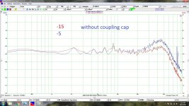
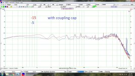
A few years back I measured the difference between the two scenarios. See attached.
Attachments
Here is the thread with a lot of good infos about the TDA :https://www.diyaudio.com/community/threads/tda1541-info.31780/
.
.
A few years back I measured the difference between the two scenarios. See attached.
Before interpreting what we see, may I enquire:
Reference point for both traces? DGND? AGND? Common Ground?
Power supply Arrangements?
Signal/sample rate supplied to TDA1541?
No output signal traces?
Past that, below 20kHz I see no systemic difference (100 sample window at high bandwidth).
Differences are above 20kHz and mainly a broad noise peak around the (presumptive) 1X sample rate and discrete spikes, ~ 78kHz on -15V (subharmonic of FDEM - FDEM/2?) and two peaks looking like mirror images of the ~78k peak around 80kHz on -5V.
Decoupling (what value capacitor) lowers noise on both lines, suggesting noise on -5V and -15V is somehow "complementary" and shorting the two points with a low enough enough impedance lowers total noise.
If so, we are back at the series connected 20V shunt regulator chain (5V+5V+10V) I have been using for several builds as the best option. In this case all currents reliably circularise, as long as a low impedance return path for Iout L+R is offered.
For modifications it suggests simply the largest value and lowest ESR Os-Con's we can find and suitable SMD cap's to a DGND plane (copper tape on kapton tape) in an L-Shape from pin 14 to pin 26 around the outside.
AGND plane (copper tape on kapton tape) in "I" shape under the IC ending at Pin 5/25 with all DEM RF decoupling Cap's (including 10nF at AOL/AOR) and -15V RF decoupling which links to DGND at pin14. This seems best practice based on multiple commercial PCB Layouts.
Thor
- Home
- Source & Line
- Digital Line Level
- Building the ultimate NOS DAC using TDA1541A