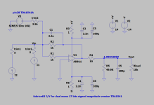
Well , things are going quite well , but I understand that staying passive all the way out is a challenge out of my reach , so next step is a new board for the DAC's , 4 layers including all the mod's and the Pedja opa 861 output stage , step by step as usual 😉
the logic board will stay the same , it works perfectly , thanks to John genius ideas and some of your tips and tricks 🙂
.
the logic board will stay the same , it works perfectly , thanks to John genius ideas and some of your tips and tricks 🙂
.
First shot of the TDA's board with 4 layers , including AD811 JRZ output :
easier than 2 layers but not that easy too
measurements of the previous board shows that staking 1 uf ceramic + 0.1 uf film at the supply's pin is ok
trimmers for the biais will remain , but the 20 ohms became 10 ohms and it will be an https://www.mouser.fr/ProductDetail/71-1280G-10-K

.
easier than 2 layers but not that easy too
measurements of the previous board shows that staking 1 uf ceramic + 0.1 uf film at the supply's pin is ok
trimmers for the biais will remain , but the 20 ohms became 10 ohms and it will be an https://www.mouser.fr/ProductDetail/71-1280G-10-K
.
Last edited:
Try to bring those dem el.capacitors closer to the chip. Perhaps even try to put some from under the board if aesthetics are not that much of concern.
the DEM cap are few mm away from de chip , FFT and scope doesn't shown any inconvenience at their level , DEM is 50Hz so nothing to worry about
different story will be DEM at 200 Khz or even more
.
different story will be DEM at 200 Khz or even more
.
@fabrice63 , with the AD811 you must use decoupling, COG and an electrolyte of at least 10uF, otherwise you could run into problems. COG must be immediately next to pins 4 and 7.
I don't understand the use of those trimmers? It turns out that no active I/V conversion is needed and that the AD811 is redundant.
I don't understand the use of those trimmers? It turns out that no active I/V conversion is needed and that the AD811 is redundant.
It may not be easy to see , but pin 4 and 7 of the AD811 ( smd type ) got their caps , 10 uf Panasonic FR + 0.1 uf ECHUX film , chips are 10 mm away from each other
trimmers are there for the biais and the equillibrium of it between the two chip , this is the "dual mono 17 bits signed magnitude version " , quite
different than a single chip setup , and as far as I dont know if it would works without biais , I'll keep it , I will easely bypass them if needed
I run the all thing on lipo battery's
.
Last edited:
I tried AD811 about 15 years ago with TDA1541 but as Walt Jung published in his article nothing like this so I am not sure about the final result and how it will work.
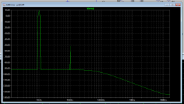
I hope I guessed the circuit as you imagined,so you get a DC voltage at the output, any noise at +5V(pin28) will be amplified in the active I/V, so you get an FFT as below in the picture. This is with 10mV/10kHz but in reality there will be HF noise that passes through the AD811 without any problems.
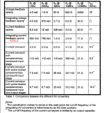
-Input Resistance of AD811 is 14ohm, so the first trimmer will surely have some influence because the active I/V is not designed with a resistor in series to input of the op amp. Until now, I have never encountered such a thing with active I/V, where the goal is for the DAC to see a resistance of 0 ohms, at least on paper. In reality Zin for AD811 is in the table.
I hope I guessed the circuit as you imagined,so you get a DC voltage at the output, any noise at +5V(pin28) will be amplified in the active I/V, so you get an FFT as below in the picture. This is with 10mV/10kHz but in reality there will be HF noise that passes through the AD811 without any problems.
-Input Resistance of AD811 is 14ohm, so the first trimmer will surely have some influence because the active I/V is not designed with a resistor in series to input of the op amp. Until now, I have never encountered such a thing with active I/V, where the goal is for the DAC to see a resistance of 0 ohms, at least on paper. In reality Zin for AD811 is in the table.
Attachments
Hi Grunf , fact is that this setup has been first created by John at post 6116 of this thread , the setup has been thought for passive output in first place , not sure it will accept active opamp output , the only one who did that is Koldby at post 7148 and beyond
the 10 ohm trim pot should remain for compensating the gain difference between the two dac's , but if I dont use the + 5 v injection there will be some DC at the dac output
may John himself give use some input about this situation 🤔
.
the 10 ohm trim pot should remain for compensating the gain difference between the two dac's , but if I dont use the + 5 v injection there will be some DC at the dac output
may John himself give use some input about this situation 🤔
.
As far as I've read, they managed to make it work with passive conversion. Trimmers are needed to zero the differences between the current outputs and the conversion is done with a resistor.
I did not include - current in my simulation so that it could avoid offset at the output, but any noise that comes from pin28 will be amplified in the active conversion and that 5V would have to come from a separate regulator.
To begin with, I would make a passive I/V as Koldby did, then maybe later try an active I/V, but I would zero the differences with a resistor in the feedback and avoid the trimmer at the input of the op amp itself. In any case you will need a precision trimmer in series with the resistor in feedback.
I wouldn't go with the AD811 right away but with some cheap op amp to start with.
I made some measurement today , here is the FFT up to 100 Khz of the noise at pin 28 +5 v while DAC is running an 1 Khz sine at 0dbv , and as Grunf says there are some stuff that will go to the AD811 , not much but still too much :
I also made the measurement of the resistance needed for the two dac's of the same chip to have their gain equalized :
1.82 ohms for one chip
1.41 ohm for the other one
it means that I can resolve the resistance seen by the AD811 at almost those value
but not sure the opamp way is the good one anyhow 🤔

.
I also made the measurement of the resistance needed for the two dac's of the same chip to have their gain equalized :
1.82 ohms for one chip
1.41 ohm for the other one
it means that I can resolve the resistance seen by the AD811 at almost those value
but not sure the opamp way is the good one anyhow 🤔
.

Well , as I am not a pro , I will stay passive all the way out as I previously said , I ordered a pair of 1495 from sowters , and I decided to give the biais circuit it's own supply , here is the routing :
View attachment 1202713
.
View attachment 1202713
.
Last edited:
https://www.diyaudio.com/community/threads/output-transformers-for-dacs.327794/Well , as I am not a pro , I will stay passive all the way out as I previously said , I ordered a pair of 1495 from sowters , and I decided to give the biais circuit it's own supply , here is the routing :
View attachment 1202713
.
Take a look here.
The point is that You should use separate Io of 2mA current injection for each output. AND separate trimming for each dac out too.Hi Grunf , fact is that this setup has been first created by John at post 6116 of this thread , the setup has been thought for passive output in first place , not sure it will accept active opamp output , the only one who did that is Koldby at post 7148 and beyond
the 10 ohm trim pot should remain for compensating the gain difference between the two dac's , but if I dont use the + 5 v injection there will be some DC at the dac output
may John himself give use some input about this situation 🤔
.
First set booth Io to 2mA, Then set the the passive R for gain. Again - the same for 0mV offset for each output. Then connect outputs and check offsett and measure...
- Home
- Source & Line
- Digital Line Level
- Building the ultimate NOS DAC using TDA1541A