It is true this simple IV transimpedance circuit performs great by just being really simple with few component counts.
What I notice however it is extremely sensitive. Any slight disturbance on either channel will effect the other.
The capacitor C1 is very important too. Any fluctuation of voltage at C1 for too fast will 'compress' the sound. The performance of C1 at high frequency will not be desirable due to large ESR. I wonder if parallel the C1 with PP cap will help.
For some reasons I cant explain, I can only use T2 =K117 in order to maintain the IDac at T1 emitter below 25mV.
I will try 1 10mH inductor before 500R and will report back.
-ecdesigns- said:Recently I derived this bias voltage from the TTL level I2S signals, so bias voltage slightly varies with duty cycle (jitter). This affects the exact moment the TDA1541A will trigger, and it can be used to compensate for timing jitter, effectively reducing sample timing jitter. It's also important to interrupt the I2S TTL level signal current flow when it drops below approx. 1V, this is required to prevent full discharge of the I2S input stray capacitance, minimizing current surges. This new I2S jitter reduction circuit has resulted in most significant increase in TDA1543 / TDA1541A sound quality since I started this project.
Hello dear EC,
I'm very curious about your further improvement in the I2S jitter reduction circuit and how would it behave in a CD-player integrated DAC...would it be possible to give some more info on this?
Thanks in advance !
I now use small 1.6VA toroidal transformers (2 x 115V primary, secondary of 2x9V are not connected). These have a DC resistance of approx. 2 K Ohm (primary windings connected in series). I connected this choke between the emitter and -12V. (so the output buffer runs on +/-12V).
I check the RS website and it didnt say about the DC resistance. Normally the DC resistance would be very low on the primary side or I am wrong. I am confused by the fact that (radial choke/induct 10mH is very low DC resistance)
Can I use this instead ?
http://my.farnell.com/block/avb3-2-2-9/transformer-3-2va-2-x-9v/dp/1131488
If I get you right, now the 500R resistor is not used. Instead just the 1.6VA encapsulated transformer connected with the 2x115V primary winding with the T2 Collector to +12V while the transformer pin to -12V ? no more 500R right.
Would appreciate if you can show the circuit for TDA1541a IV single ended circuit.
experimental M1.
After my CD PRO low DATA output (100mV , 200mV) refused to stimulate the lonely TDA1543 DAC chip to produce music, I built a pretty floating charge transfer supply and put together an M1 under less than optimal conditions > thanks that I always use a Variac to try new projects since I forgot that the final cap of the floating charge transfer supply sees double the V.
I had to swap the original transformer for a smaller one, because the PS caps would not take the high V, so the V regulator are now not optimally fed...nevertheless, the little M1 DAC with the stock transistor single ended trans/impedance (triple BC550 in my case) circuit and lower than recommended DC blocking Claritycaps, sounds not bad at all...
Next I will install an appropriate transformer and try one of my 4 DAC towers... 😀
Shall I lower I/V R to 1/4, from 2K5 and increase the output cap accordingly?
For my CD PRO I plan to build a signal transformer to increase x4 the voltage of DATA signal.
Regards,
M
PS. I will try to post a pick, if and when the daughters lend me their camera... 🙁
I wonder for the transimpedance circuit, placing the choke 10mH in series with 500R resistor works like a high pass ? or the 500R is there to bias the T2 and hold the output for the 'Headroom'
The f-3dB is determine by the 1/2xpixRxL ? and practically the f-3dB should be 10 times lower then the 20Hz region right ?
The f-3dB is determine by the 1/2xpixRxL ? and practically the f-3dB should be 10 times lower then the 20Hz region right ?
My humble D1M.
Floating charge transfer has BDX33/44C. USB module has common type 12M clock. No I2S attenuation for the +/- 2V digital signals from PCM2707, yet...
http://picasaweb.google.com/lh/photo/_K9J85aQ8OHnqbQkbZ_PYw?feat=directlink
Regards,
M
Floating charge transfer has BDX33/44C. USB module has common type 12M clock. No I2S attenuation for the +/- 2V digital signals from PCM2707, yet...
http://picasaweb.google.com/lh/photo/_K9J85aQ8OHnqbQkbZ_PYw?feat=directlink
Regards,
M
Re: hi cschua
pls try ebay. search for tda1541a. follow ecdesign mod will do.
Pocoyo said:where you found your dacs ?
what mods already done ? Listing please
pls try ebay. search for tda1541a. follow ecdesign mod will do.
Manage to try out the Ibias at the T1 output. I set the Ibias at 40uA using 300K0 resistor tied to -12V dc. The Idac at T1 Emitter is found to be -1.0mV quite consistently.
The feeling is mixed. It is not 'big difference' but certainly more enjoyable having the Ibias. Higher Ibias at 120uA is not good.
The feeling is mixed. It is not 'big difference' but certainly more enjoyable having the Ibias. Higher Ibias at 120uA is not good.
Hi,
I am coming too late (?) and - sorry - I cannot recognize the actual state of development. I have two questions:
- sound
Can someone say anything about the sound of this promising project, compared to Altmanns...?
- PCBs
Are there still ready PCBs or Kits?
Thanks a lot.
Regards
Thomas
I am coming too late (?) and - sorry
- I cannot recognize the actual state of development. I have two questions:- sound
Can someone say anything about the sound of this promising project, compared to Altmanns...?
- PCBs
Are there still ready PCBs or Kits?
Thanks a lot.
Regards
Thomas
I really hope ECDesigns can come out with the most optimized layout of the tDA 1541a.
The sound of TDA1541a easily beats the new DAC chip currently on market.
I still prefer to operate the transimpedance circuit with 700mV reverse bias on the T2. This is because when Idac goes to 0mA, the output of Collector and Base of T2 goes into saturation.
The sound of TDA1541a easily beats the new DAC chip currently on market.
I still prefer to operate the transimpedance circuit with 700mV reverse bias on the T2. This is because when Idac goes to 0mA, the output of Collector and Base of T2 goes into saturation.
The sound of TDA1541a easily beats the new DAC chip currently on market.
The "sound" of any chip doesn't make the sound of a whole DAC. There is a little bit more on it. That is the reason for my question... 🙂
Hi EC,
I put the right (2x9V) R-core transformer and also installed cheap non-polar 33uF output caps parallel my ClarityCaps (3.9uF) on my experimental D1M and the sound improved significantly.
I like it! 🙂
The floating charge transfer supply seem to work great.
I wait for your digital input modules...
Regards,
M
Hi John,
i also tried DEM mod and works and sounds really great!
It makes quite big diffence in sound. I would say more organic or natural sound.
Thanks a lot.
Bostjan
i also tried DEM mod and works and sounds really great!
It makes quite big diffence in sound. I would say more organic or natural sound.
Thanks a lot.
Bostjan
Hi TJF,
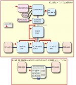
It's difficult to compare DAC performance when the DACs use different interface types, are connected to different digital audio sources, amplifiers and speakers.
All I can say is that the digital audio source and sample timing will determine how a DAC performs. I personally think that the only way to get ultimate performance is to integrate a suitable digital audio source in the DAC (same housing), and using I2S interface.
If you also want to hear actual DAC resolution, you will need to re-arrange the signal flow through a conventional audio set.
It basically means driving the power amplifier at maximum amplitude (0dB on the recording results in maximum signal amplitude at the amplifier output), and placing a variable power series resistor (stepped) between speaker interlink and speaker.
This will greatly improve S/N ratio and reduce audible (crossover) distortion. The result is maximum resolution, regardless of volume setting.
DI16 and DI8M PCBs are available, the new projects are still under development.
I am coming too late (?) and - sorry - I cannot recognize the actual state of development. I have two questions:
- sound
Can someone say anything about the sound of this promising project, compared to Altmanns...?
It's difficult to compare DAC performance when the DACs use different interface types, are connected to different digital audio sources, amplifiers and speakers.
All I can say is that the digital audio source and sample timing will determine how a DAC performs. I personally think that the only way to get ultimate performance is to integrate a suitable digital audio source in the DAC (same housing), and using I2S interface.
If you also want to hear actual DAC resolution, you will need to re-arrange the signal flow through a conventional audio set.
It basically means driving the power amplifier at maximum amplitude (0dB on the recording results in maximum signal amplitude at the amplifier output), and placing a variable power series resistor (stepped) between speaker interlink and speaker.
This will greatly improve S/N ratio and reduce audible (crossover) distortion. The result is maximum resolution, regardless of volume setting.
- PCBs
Are there still ready PCBs or Kits?
DI16 and DI8M PCBs are available, the new projects are still under development.
for the charge transfer, can I know why is the meaning of the green shaded area ?
In order to connect the floating charge transfer to the Transimpedance circuit, can I assume +12 to the positive terminal and ground to the negative terminal of charge transfer. In this way, the output RCA ground is also connected to the negative terminal right.
In order to connect the floating charge transfer to the Transimpedance circuit, can I assume +12 to the positive terminal and ground to the negative terminal of charge transfer. In this way, the output RCA ground is also connected to the negative terminal right.
Hi ecdesigns,
thank you for your statement!
That is shurely consequent. But I cannot integrate sources (i.e. PC) in one housing. Because of the longer cables, what is a problem with I2S, this is not practicabel for me to use it. I am using 850nm Fiber LEDs and the next days 1310 nm singlemode FP-Laser transmitter and receiver for digital signal transport will arrive. But this way of complete galvanic isolation with superior effect - compared to the usual S/PDIF solutions - needs also any kind of jitter treatment as Altmann does. Even with I2S that problem still exists. Here a usefull link to interfaces
I've seen your very promising DI-16 project, but I think that isn't my way (s. above) ... 🙁
Best regards
Thomas
thank you for your statement!
is to integrate a suitable digital audio source in the DAC (same housing), and using I2S interface.
That is shurely consequent. But I cannot integrate sources (i.e. PC) in one housing. Because of the longer cables, what is a problem with I2S, this is not practicabel for me to use it. I am using 850nm Fiber LEDs and the next days 1310 nm singlemode FP-Laser transmitter and receiver for digital signal transport will arrive. But this way of complete galvanic isolation with superior effect - compared to the usual S/PDIF solutions - needs also any kind of jitter treatment as Altmann does. Even with I2S that problem still exists. Here a usefull link to interfaces
I've seen your very promising DI-16 project, but I think that isn't my way (s. above) ... 🙁
Best regards
Thomas
-ecdesigns- said:Hi ccschua,
I now use small 1.6VA toroidal transformers (2 x 115V primary, secondary of 2x9V are not connected). These have a DC resistance of approx. 2 K Ohm (primary windings connected in series). I connected this choke between the emitter and -12V. (so the output buffer runs on +/-12V). This saves buying a 500R bulk metal foil, and sounds much better.
Others may be suitable as well, so you could experiment with different types. Best would be small safety-transformers that have an air-gap for protection against short-circuit. These don't require a fuse, when short-circuit, power is limited by the air gap. The presence of this air gap prevents possible core saturation.
Hi ECDesigns,
I dont seem to get it.
The DC resistance of 1.6VA with the secondary open according the specs seem to be less than 2kohm. typically they are less than 600ohm ?
If this transformer is less than 600ohm, now if this transformer is connected to T2 emitter and -12V, the power across it is much higher causing overheating.
Further, with the trasnformer secondary in open circuit, the primary can be modeled as having a resistor and inductor in parallel. This seem to be different than the original circuit where the inductor is in series to the resistor.
Kindly enlighten.
after much tweaking, I found putting a audio grade air core inductor in series with the 500R transimpedance gives more neutral sounding. The inductor is a Jantzen 0.2mH with 0.19 ohm DC resistance and it is not expensive but occupy lots of space.
Putting that inductors puts more focus to the music.
The output cap is Solen fastcap bypass with Roederstein 1837.
I have ordered the Vishay precision resistor together with Mundorf supreme coupling cap from Partsconnexion. waiting for arrival. Next to try is the charge transfer. Not sure where to connect the ground pin.
- Home
- Source & Line
- Digital Line Level
- Building the ultimate NOS DAC using TDA1541A