-ecdesigns- said:
I plan to go for 2 final designs, first is a simple low-cost DAC with integrated SD-card player that should provide very high perceived sound quality (better than DI8M, DI4T, or D1M).
great news EC,
pls also consider adding to it FLAC reading ability in near future if you can,...this would be a real improvement because lots of people are archiving their CD collection on HDD/DVD in this format and they may be too lazy to re-convert them to wav 😀
ps.
i also think just an SD card player with I2S output would be more than welcome since many people have already their own DIY or commercial DACs so they would only need a good digital source for them
This will drive a (multi-segmented) high-voltage trans-impedance / power buffer stage that produces approx 60 ... 70Vpp in 8 Ohms.
70vpp is enough to drive the grid of many DHTs, such as 2A3 and 300B. So, maybe if there is a low current output version of your output state, tube diehards can use their DHTs and output transformers as well.
a333bt said:
This one would be my dream!
All in one box.
Very practical and sound wise!
Less cables, connectors, housings...
I already waiting for that!
Best regards,
Bostjan
That was what I was saying. It is a great idea.
I would like to make a balanced power buffer

Hi agent.5
This is no problem at all, just use T1 and tap the signal directly from the I/V resistor (provided load impedance is high enough, and capacitive load is low enough). It's relatively easy to generate even higher ac output voltages, this basically depends on trans-impedance converter power supply and Vce voltage of T1. I already achieved approx. 90Vpp with a single TDA1543 and 10 x 9V battery in series.
In order to get 70Vpp, the following I/V resistor values are required:
1 x TDA1543, 30K4,
2 x TDA1543, 15K2
4 x TDA1543, 7K6
8 x TDA1543, 3K8
1 x TDA1541A, 17K5
2 x TDA1541A, 8K7
4 x TDA1541A, 4K37
8 x TDA1541A, 2K19
I/V resistor value can be varied for achieving volume control, this way the DAC produces exactly the required amplitude, skipping the conventional volume control.
70vpp is enough to drive the grid of many DHTs, such as 2A3 and 300B. So, maybe if there is a low current output version of your output state, tube diehards can use their DHTs and output transformers as well.
This is no problem at all, just use T1 and tap the signal directly from the I/V resistor (provided load impedance is high enough, and capacitive load is low enough). It's relatively easy to generate even higher ac output voltages, this basically depends on trans-impedance converter power supply and Vce voltage of T1. I already achieved approx. 90Vpp with a single TDA1543 and 10 x 9V battery in series.
In order to get 70Vpp, the following I/V resistor values are required:
1 x TDA1543, 30K4,
2 x TDA1543, 15K2
4 x TDA1543, 7K6
8 x TDA1543, 3K8
1 x TDA1541A, 17K5
2 x TDA1541A, 8K7
4 x TDA1541A, 4K37
8 x TDA1541A, 2K19
I/V resistor value can be varied for achieving volume control, this way the DAC produces exactly the required amplitude, skipping the conventional volume control.
Hi EC
Speaking of batteries, have you tried 1.5V small batteries (AAA) for the bias voltage on the I2S attenuators?
Thanks
JimS
Speaking of batteries, have you tried 1.5V small batteries (AAA) for the bias voltage on the I2S attenuators?
Thanks
JimS
Hi jims,
I use quite a different circuit now, it dynamically shifts trigger level threshold to compensate for BCK timing jitter. The (5V) power supply is no longer required.
> When using jittery clock signals, keeping trigger level constant, it results in sample timing jitter.
> When using a zero jitter clock signal and a non-constant trigger level (noise, hum), it results in sample timing jitter.
> But if the DAC chip trigger level is being dynamically varied in order to compensate for clock jitter, sample timing jitter can be further reduced, (theoretically to almost zero).
Clock signal jitter is basically a form of phase modulation (duty cycle variation) that can be translated to minute voltage fluctuations.
These voltage fluctuations can be used to slightly change the moment the DAC chip electronics trigger (slightly earlier or later), effectively compensating for sample timing jitter, despite presence of clock jitter. In other words, the sample jitter can be lower than the bit (master clock) jitter when dynamic trigger threshold compensation is used.
The now much lower sample jitter amplitude can be further optimized by injecting very low level white noise (noise produced by a semiconductor for example), this will result in a flatter residual jitter frequency spectrum.
I am currently testing such a circuit on both D1 and D1M DACs.
Speaking of batteries, have you tried 1.5V small batteries (AAA) for the bias voltage on the I2S attenuators?
I use quite a different circuit now, it dynamically shifts trigger level threshold to compensate for BCK timing jitter. The (5V) power supply is no longer required.
> When using jittery clock signals, keeping trigger level constant, it results in sample timing jitter.
> When using a zero jitter clock signal and a non-constant trigger level (noise, hum), it results in sample timing jitter.
> But if the DAC chip trigger level is being dynamically varied in order to compensate for clock jitter, sample timing jitter can be further reduced, (theoretically to almost zero).
Clock signal jitter is basically a form of phase modulation (duty cycle variation) that can be translated to minute voltage fluctuations.
These voltage fluctuations can be used to slightly change the moment the DAC chip electronics trigger (slightly earlier or later), effectively compensating for sample timing jitter, despite presence of clock jitter. In other words, the sample jitter can be lower than the bit (master clock) jitter when dynamic trigger threshold compensation is used.
The now much lower sample jitter amplitude can be further optimized by injecting very low level white noise (noise produced by a semiconductor for example), this will result in a flatter residual jitter frequency spectrum.
I am currently testing such a circuit on both D1 and D1M DACs.
Thanks for the explanation. So you are using the phase comparator in the PLL to accomplish this. Does the jitter in the reference and the input signal have to be identical for this to work?
Still do not understand why the injection of pink noise would further reduce the signal
JimS
Still do not understand why the injection of pink noise would further reduce the signal
JimS
Hi jims,
No, its integrated in the BCK attenuator (passive circuit), it creates a dynamically varying bias voltage. The bias voltage amplitude varies ever so slightly with bit clock phase fluctuations (timing jitter). Noise produced by diodes is used to inject very low level noise. By dynamically increasing / decreasing the bias voltage, and given the finite BCK transient time, it's possible to force the DAC chip to trigger slightly earlier or later (depending on bit clock jitter). This results in reduced sample timing jitter at the DAC analogue outputs (bit clock jitter remains unchanged).
Note that these are barely measurable bias voltage fluctuations, as these only need to make corrections in the ps range.
Apart from sample jitter amplitude (that cannot be reduced to zero), resulting jitter spectrum will continue to affect performance. Altmann designed the Jisco jitter decorrelator that does something similar.
But this isn't all.
There is basically no difference between analogue output sample timing jitter being caused by master clock jitter, or by phase distortion / interference induced by connected analogue circuits. In both cases the result is increased analogue sample timing jitter.
In other words, even if the DAC manages to output analogue sample values with very low analogue sample timing jitter, the connected analogue circuit can still mess things up badly, resulting in .... analogue sample timing jitter.
So there are multiple sources for jitter induced sound quality degradation, the master clock jitter is only one of many.
That's why I now plan to use following:
SD-card player (very low master clock jitter to start with) > dynamic jitter attenuator > DAC chip > large bandwidth I/V converter > large bandwidth power buffer > speakers (pre-filtering) > human auditory system (brickwall filtering).
So I perform filtering at the end of the audio signal path in order to avoid accumulated (phase) errors.
So you are using the phase comparator in the PLL to accomplish this
No, its integrated in the BCK attenuator (passive circuit), it creates a dynamically varying bias voltage. The bias voltage amplitude varies ever so slightly with bit clock phase fluctuations (timing jitter). Noise produced by diodes is used to inject very low level noise. By dynamically increasing / decreasing the bias voltage, and given the finite BCK transient time, it's possible to force the DAC chip to trigger slightly earlier or later (depending on bit clock jitter). This results in reduced sample timing jitter at the DAC analogue outputs (bit clock jitter remains unchanged).
Note that these are barely measurable bias voltage fluctuations, as these only need to make corrections in the ps range.
Still do not understand why the injection of pink noise would further reduce the signal
Apart from sample jitter amplitude (that cannot be reduced to zero), resulting jitter spectrum will continue to affect performance. Altmann designed the Jisco jitter decorrelator that does something similar.
But this isn't all.
There is basically no difference between analogue output sample timing jitter being caused by master clock jitter, or by phase distortion / interference induced by connected analogue circuits. In both cases the result is increased analogue sample timing jitter.
In other words, even if the DAC manages to output analogue sample values with very low analogue sample timing jitter, the connected analogue circuit can still mess things up badly, resulting in .... analogue sample timing jitter.
So there are multiple sources for jitter induced sound quality degradation, the master clock jitter is only one of many.
That's why I now plan to use following:
SD-card player (very low master clock jitter to start with) > dynamic jitter attenuator > DAC chip > large bandwidth I/V converter > large bandwidth power buffer > speakers (pre-filtering) > human auditory system (brickwall filtering).
So I perform filtering at the end of the audio signal path in order to avoid accumulated (phase) errors.
Dear John EC,
The DEM clock circuit consists of two resistive attenuators that perform biasing, level-shifting and attenuation. The DEM clock frequency has been increased to 2.8224 MHz (bit clock).
I modified the DI8M with 2.8224 Mhz DEM clock
In the timing chain U11 (74hct161) is removed
BCKT (pin 2) on socket wire bridged to DCLK Dem out (pin 12)
From DCLK to a DS 8921 (as in my earlier mod post 2535)
From DS 8921 via your circuit 2 x 10K + out to PIN 17 - out to pin 16 and 2x 2k2 to pin 15 (= - 15v) on mudule TDA1541a number 1
and - out to pin 17 + out to pin 16 on the modules 2-8.
(2-8 have inverted BCK !)
The result is IMO (after 24 hours solder rest) the best improving mod for this DAC I did !
John
Thanks again for sharing this DEM invention.
Best Regards,
Onno
HI ECDesigns,
for the coupling cap at the transimpedance circuit, since 4.7uF VCAP TFTF would be cost prohibitive, is it possible to use 0.22uF with 220k drain resistor. In this way, the F at 3dB still within the 20hz band but will this increase the phase distortion at low freq?
for the coupling cap at the transimpedance circuit, since 4.7uF VCAP TFTF would be cost prohibitive, is it possible to use 0.22uF with 220k drain resistor. In this way, the F at 3dB still within the 20hz band but will this increase the phase distortion at low freq?
-ecdesigns- said:
The ultimate design will probably be a direct-drive DAC, it's a "single-box" solution that has a SD-card player as source. I will probably require 4 x TDA1541A for boosting DAC full-scale current to 16mA. This will drive a (multi-segmented) high-voltage trans-impedance / power buffer stage that produces approx 60 ... 70Vpp in 8 Ohms. Integrated volume control will probably be done by varying the passive I/V resistor value.
This DAC will be different from all previous designs, as the problematic pre-amp, power-amp and volume control are simply eliminated too. This DAC directly drives the speakers! Recent test setups (20Vpp) showed dramatic improvements in sound quality, it illustrates how much performance is actually lost during subsequent attenuation (volume control) and power amplification. This is backed-up by measurements performed at the power amplifier output.
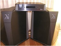
Something like Wadia's Power Dac?
With all respect, John... But did you actually listen to the Zanden 2000p transport and 5000 mk3 dac combi?
rgrds
Anton.
Attachments
scrutinizer said:
Something like Wadia's Power Dac?
With all respect, John... But did you actually listen to the Zanden 2000p transport and 5000 mk3 dac combi?
rgrds
Anton.
Dear Anton
I bed you work for Symphony Audio Import BV or one of its dealers

But as you are living in Rotterdam, you are welkome to my place to listen to one of John' s dacs and bring the Zanden with you to compare.
Onno
Hi Onno,
[.....]😱
No disrespect, just a question that is of some importance for validation ... that's all.
I can only say that if Yamada (Zanden) makes this possible with a TDA 1541 "gold crown", I'm curious to know how John's 'voiced' Dac will 'sound' like.
And for your other questions..... Worked with them .... know the products .... 'listen' to them for a while .... but 'still' have a hobby.
That's my reason for joining this forum .... as is yours I presume 😉
regards,
Anton.
[.....]😱
No disrespect, just a question that is of some importance for validation ... that's all.
Based on the technical information I was able to collect about the van Zanden 5000 Mk.IV, I am pretty confident that the DI 8M will be able to outperform it.
I can only say that if Yamada (Zanden) makes this possible with a TDA 1541 "gold crown", I'm curious to know how John's 'voiced' Dac will 'sound' like.
And for your other questions..... Worked with them .... know the products .... 'listen' to them for a while .... but 'still' have a hobby.
That's my reason for joining this forum .... as is yours I presume 😉
regards,
Anton.
So could it be possible to tune (linearize) the 6 MSBs of a TDA1541A by injecting adjustable constant currents at the decoupling pins? A perspective of converting a plain 1541 into double crown, triple crown..-ecdesigns- said:Current sources may be perfect in a simulation, but in practice there is significant (power supply) pollution present that's extremely difficult to reduce to required nV / nA region. The simple constant current sources, based on a JFET are far from perfect and output current still varies with power supply voltage fluctuations.
You can easily test this by attempting to tune TDA1541A bit errors by feeding an external constant current into the active divider decoupling pins, and these are only the 6 MSBs!
Hi oshifis,
I attached part of the TDA1540 internal schematics (IEEE JOURNAL OF SOLID-STATE CIRCUITS, VOL. SC-14, NO. 3, JUNE 1979). TDA1541A schematics are similar, but this one has 10 passive current dividers and 6 active current dividers.
On the top right there is the current reference source, all binary weighted bit currents are derived (divided) from this reference current source. So if the output current of this current source changes (drift), all bit currents will change accordingly, preserving bit accuracy.
This constant current source also directly provides MSB current (2mA). It's mirrored against -15V, and then enters the first active divider (not shown).
There are 3 active dividers visible, they are driven through shift-register outputs A, B, C, and D. The speed the shift register is clocked, is determined by the DEM clock frequency.
Each active current divider consists of 4 transistors (passive divider) supplying 4 coarse (almost equal) currents to the switching matrix. The switching matrix connects each active divider output to each passive divider output alternatively, using a specific switching pattern. This way the active dividers perform time-averaging, meaning that the active divider outputs derive 4 closely matched output currents from 4 not so closely matched input currents. Two of these outputs are always tied together:
Example:
Input currents, 0.51mA, 0.48mA, 0.46mA, 0.49mA. After time averaging, 4 output currents are derived, each of these output currents equals (0.51 + 0.48 + 0.46 + 0.49) / 4 = 0.485mA. Since 2 outputs are connected, the output currents are 0.485mA, 0.485mA, and 0.97mA.
In other words, despite tolerances in the 4 passive divider input currents, the derived output currents will be closely matched due to time averaging. The currents are dynamically tuned to close tolerances.
There is a catch, if the time intervals between switching (DEM clock) vary, for example 5us, 0.49us, 5.1us, and 0.48uS, the passive divider tolerances aren't fully corrected, and bit errors occur. That's why it's important to keep the DEM clock jitter as low as possible as DEM clock jitter might result in higher bit errors.
Back to the TDA1541A-S2, running on the standard free running jittery DEM clock that prevents close matching of the 4 input currents. The only way to still get closely matched currents at the active divider output is to have equally close matched outputs on the passive dividers. Using above example:
Input currents, 0.485mA, 0.485mA, 0.485mA, 0.485mA. After time averaging (time intervals aren't equal), the output currents are still 0.485, 0.485, 0.485, 0.485.
The MSBs will have biggest impact on bit errors, the slightest errors here, and accuracy degrades quickly.
So the TDA1541A-S2 is only a plain TDA1541A that has slightly closer matching of the passive dividers that feed the switching matrix. So with the given jittery DEM clock, it still manages to provide slightly higher bit accuracy. But much more important, it will have lower ripple current on the active divider outputs too.
On the other hand, when we feed a plain TDA1541A chip with a highly accurate, low-jitter DEM clock that runs in sync with BCK, all DEM clock time intervals will be closely matched. This will result in similar performance as the S2 chip with closer passive divider current matching.
Passive divider tolerances also translate to increased ripple current on the active divider outputs. These outputs are filtered using an internal resistor, and an external decoupling capacitor (marked red).
The bigger the passive divider tolerances, the higher the ripple current amplitude. In order to prevent this, the DEM clock can be increased by approx. factor 10 (from approx. 200KHz to approx. 2.8224 MHz). Now it's easier to filter the active divider outputs and reduce ripple current (noise).
So TDA1541A performance can be significantly increased by ensuring DEM clock jitter is very low (equal time intervals), and DEM clock switching frequency is significantly increased (lower ripple current). Max. DEM clock frequency is limited to approx. 7 MHz,
Other factor that increases output current noise levels are the I2S signals. Even minute voltage fluctuations (ground-bounce) can affect the highly sensitive output signal. And since I/V conversion has to take place sooner or later, noise on the GND reference will degrade accuracy.
This is why it's very important to take whatever measures to minimize I2S induced ground-bounce. On chip, high-speed current steering logic is used (+/- 400mV levels), so here interference is already minimized.
In practice this means reducing I2S signal levels to approx. 400 ...600mVpp levels. The I2S inputs require a bias voltage of approx. 1 ... 1.4V, so this bias voltage has to be provided too. Using the SD-card player, it's possible to lower ground-bounce even further by using 32 bits / frame, resulting in 1.4112 MHz bit clock (ground-bounce decreases with decreased voltage and decreased frequency).
Recently I derived this bias voltage from the TTL level I2S signals, so bias voltage slightly varies with duty cycle (jitter). This affects the exact moment the TDA1541A will trigger, and it can be used to compensate for timing jitter, effectively reducing sample timing jitter. It's also important to interrupt the I2S TTL level signal current flow when it drops below approx. 1V, this is required to prevent full discharge of the I2S input stray capacitance, minimizing current surges. This new I2S jitter reduction circuit has resulted in most significant increase in TDA1543 / TDA1541A sound quality since I started this project.
So could it be possible to tune (linearize) the 6 MSBs of a TDA1541A by injecting adjustable constant currents at the decoupling pins? A perspective of converting a plain 1541 into double crown, triple crown..
I attached part of the TDA1540 internal schematics (IEEE JOURNAL OF SOLID-STATE CIRCUITS, VOL. SC-14, NO. 3, JUNE 1979). TDA1541A schematics are similar, but this one has 10 passive current dividers and 6 active current dividers.
On the top right there is the current reference source, all binary weighted bit currents are derived (divided) from this reference current source. So if the output current of this current source changes (drift), all bit currents will change accordingly, preserving bit accuracy.
This constant current source also directly provides MSB current (2mA). It's mirrored against -15V, and then enters the first active divider (not shown).
There are 3 active dividers visible, they are driven through shift-register outputs A, B, C, and D. The speed the shift register is clocked, is determined by the DEM clock frequency.
Each active current divider consists of 4 transistors (passive divider) supplying 4 coarse (almost equal) currents to the switching matrix. The switching matrix connects each active divider output to each passive divider output alternatively, using a specific switching pattern. This way the active dividers perform time-averaging, meaning that the active divider outputs derive 4 closely matched output currents from 4 not so closely matched input currents. Two of these outputs are always tied together:
Example:
Input currents, 0.51mA, 0.48mA, 0.46mA, 0.49mA. After time averaging, 4 output currents are derived, each of these output currents equals (0.51 + 0.48 + 0.46 + 0.49) / 4 = 0.485mA. Since 2 outputs are connected, the output currents are 0.485mA, 0.485mA, and 0.97mA.
In other words, despite tolerances in the 4 passive divider input currents, the derived output currents will be closely matched due to time averaging. The currents are dynamically tuned to close tolerances.
There is a catch, if the time intervals between switching (DEM clock) vary, for example 5us, 0.49us, 5.1us, and 0.48uS, the passive divider tolerances aren't fully corrected, and bit errors occur. That's why it's important to keep the DEM clock jitter as low as possible as DEM clock jitter might result in higher bit errors.
Back to the TDA1541A-S2, running on the standard free running jittery DEM clock that prevents close matching of the 4 input currents. The only way to still get closely matched currents at the active divider output is to have equally close matched outputs on the passive dividers. Using above example:
Input currents, 0.485mA, 0.485mA, 0.485mA, 0.485mA. After time averaging (time intervals aren't equal), the output currents are still 0.485, 0.485, 0.485, 0.485.
The MSBs will have biggest impact on bit errors, the slightest errors here, and accuracy degrades quickly.
So the TDA1541A-S2 is only a plain TDA1541A that has slightly closer matching of the passive dividers that feed the switching matrix. So with the given jittery DEM clock, it still manages to provide slightly higher bit accuracy. But much more important, it will have lower ripple current on the active divider outputs too.
On the other hand, when we feed a plain TDA1541A chip with a highly accurate, low-jitter DEM clock that runs in sync with BCK, all DEM clock time intervals will be closely matched. This will result in similar performance as the S2 chip with closer passive divider current matching.
Passive divider tolerances also translate to increased ripple current on the active divider outputs. These outputs are filtered using an internal resistor, and an external decoupling capacitor (marked red).
The bigger the passive divider tolerances, the higher the ripple current amplitude. In order to prevent this, the DEM clock can be increased by approx. factor 10 (from approx. 200KHz to approx. 2.8224 MHz). Now it's easier to filter the active divider outputs and reduce ripple current (noise).
So TDA1541A performance can be significantly increased by ensuring DEM clock jitter is very low (equal time intervals), and DEM clock switching frequency is significantly increased (lower ripple current). Max. DEM clock frequency is limited to approx. 7 MHz,
Other factor that increases output current noise levels are the I2S signals. Even minute voltage fluctuations (ground-bounce) can affect the highly sensitive output signal. And since I/V conversion has to take place sooner or later, noise on the GND reference will degrade accuracy.
This is why it's very important to take whatever measures to minimize I2S induced ground-bounce. On chip, high-speed current steering logic is used (+/- 400mV levels), so here interference is already minimized.
In practice this means reducing I2S signal levels to approx. 400 ...600mVpp levels. The I2S inputs require a bias voltage of approx. 1 ... 1.4V, so this bias voltage has to be provided too. Using the SD-card player, it's possible to lower ground-bounce even further by using 32 bits / frame, resulting in 1.4112 MHz bit clock (ground-bounce decreases with decreased voltage and decreased frequency).
Recently I derived this bias voltage from the TTL level I2S signals, so bias voltage slightly varies with duty cycle (jitter). This affects the exact moment the TDA1541A will trigger, and it can be used to compensate for timing jitter, effectively reducing sample timing jitter. It's also important to interrupt the I2S TTL level signal current flow when it drops below approx. 1V, this is required to prevent full discharge of the I2S input stray capacitance, minimizing current surges. This new I2S jitter reduction circuit has resulted in most significant increase in TDA1543 / TDA1541A sound quality since I started this project.
Attachments

To ECDesigns,
Shall I call your latest DEM reclocking the ultimate, or is there more to come.
After listening to it for 15 minute (normally my listening session is 1 hour), I cant wait to drop back to write my appreciation for this inventions.
It has the effects like changing my output cap to VCAP. It is really neutral and the sound of cymbals is really accurate now. The bass attack has weight and carry through.
Thanks.
me too,my whole appreciation for EC for sharing with us his knowledge and his great findings !
For the transimpedance circuit, I notice ECDesign had used both I/V resistor and 510R as Vishay S102J.
It is difficult to obtain S102J in 1.5k ohm and I know this precision resistor sound the best in the world in terms of most neutral and least grain. Can I know instead of S102J, is the Vishay VTA54/52 series also acceptable ?
The Temp coef is quite good and the pricess is cheaper (the tolereance not as good)
Hi ccschua,
Try Percy Audio for "special" bulk metal foil resistor values. Use this resistor for I/V conversion only.
The output stage appears to work best when loaded with a choke. Push-pull, (cascoded) current source, and many other configurations failed to achieve the clarity produced by a choke-loaded SE buffer, and produced much higher measurable noise levels at the buffer output. I now use small 1.6VA toroidal transformers (2 x 115V primary, secondary of 2x9V are not connected). These have a DC resistance of approx. 2 K Ohm (primary windings connected in series). I connected this choke between the emitter and -12V. (so the output buffer runs on +/-12V). This saves buying a 500R bulk metal foil, and sounds much better.
The transformers are available from RS components, P/N 223-8998 (2 x 9V, 1.8VA).
Others may be suitable as well, so you could experiment with different types. Best would be small safety-transformers that have an air-gap for protection against short-circuit. These don't require a fuse, when short-circuit, power is limited by the air gap. The presence of this air gap prevents possible core saturation.
It is difficult to obtain S102J in 1.5k ohm and I know this precision resistor sound the best in the world in terms of most neutral and least grain. Can I know instead of S102J, is the Vishay VTA54/52 series also acceptable ?
Try Percy Audio for "special" bulk metal foil resistor values. Use this resistor for I/V conversion only.
The output stage appears to work best when loaded with a choke. Push-pull, (cascoded) current source, and many other configurations failed to achieve the clarity produced by a choke-loaded SE buffer, and produced much higher measurable noise levels at the buffer output. I now use small 1.6VA toroidal transformers (2 x 115V primary, secondary of 2x9V are not connected). These have a DC resistance of approx. 2 K Ohm (primary windings connected in series). I connected this choke between the emitter and -12V. (so the output buffer runs on +/-12V). This saves buying a 500R bulk metal foil, and sounds much better.
The transformers are available from RS components, P/N 223-8998 (2 x 9V, 1.8VA).
Others may be suitable as well, so you could experiment with different types. Best would be small safety-transformers that have an air-gap for protection against short-circuit. These don't require a fuse, when short-circuit, power is limited by the air gap. The presence of this air gap prevents possible core saturation.
- Home
- Source & Line
- Digital Line Level
- Building the ultimate NOS DAC using TDA1541A