-ecdesigns- said:
This configuration works with moderate output voltages across the I/V resistor (limited power provided by the single DAC chip). Since there is no attenuation (variable I/V resistor), sound is really crystal clear, free of distortion and noise that's so typical with subsequent attenuation (volume control), and amplification (power amp).
If 10 ... 20 watts rms is sufficient, this is a super solution. You just have to include protection circuits to prevent loud pops or clicks during power-up, power-down, and when using resistors and switches for varying I/V resistor value.
When using a single TDA1543, you will need approx. 12K Ohm I/V resistor for 10W rms, and approx. 24K Ohm resistor for 20W rms (using a unity-gain power buffer). The use of the trans-impedance stage is required here, so TDA1543 25mVpp output compliance is fully met.
The trans-impedance I/V converter / buffer uses no active amplification ? I already read about 2V output without any active stage but only 25mVpp on the TDA1543, that sounds a bit mysterious to me.
How do you do that ?
And that ?:
24K Ohm resistor for 20W rms
Hi Bernhard,
It's no problem to drive 8 bit clock loads, it's a problem maintaining extreme low bit clock jitter while driving these loads.
I mentioned that the I/V resistor is not connected directly to the DAC chip output.
Take a NPN transistor, emitter goes to TDA1543 current output, basis goes to 2.7V reference voltage, and the I/V resistor is connected between collector and a positive voltage that's high enough for desired ac voltage across this I/V resistor.
This way, max. ac voltage at the TDA1543 current output is approx. 5mV max (approx. 2 Ohm load impedance), while the ac voltage across the I/V resistor can be way higher. I managed to get 90Vpp across a 39 K Ohm I/V resistor and a power supply of 100 volts.
I used a 2K5 I/V resistor in the D1M, with TDA1543 2.3mA full scale current this generates .0023 x 2500 = 5.75Vpp or 2.03V rms. The ac voltage across the I/V resistor is buffered of course.
Sorry my mistake. With 24K Ohm I/V resistor, a single TDA1543 will output 0.0023 x 24,000 = 55.2Vpp or 19.52V rms. The power supply for the I/V resistor should be around 60 Volts. This voltage is high enough to drive a unity gain power buffer. The power buffer then drives the speaker. Using 24 K Ohm I/V resistor, output power into an 8 Ohm load equals (19.2 x 19.2) / 8 = 46 watts rms.
The idea is to prevent subsequent attenuation (volume control) and amplification (power amp), by generating just the right signal amplitude in the DAC. This can be done using a variable I/V resistor.
When I tried to drive 8 paralleled bit clock inputs over a longer distance directly from CS8412, there was a crackling noise and 330 ohm termination was needed to avoid that.
With my opamp based clock buffer it works well without termination.
It's no problem to drive 8 bit clock loads, it's a problem maintaining extreme low bit clock jitter while driving these loads.
The trans-impedance I/V converter / buffer uses no active amplification ? I already read about 2V output without any active stage but only 25mVpp on the TDA1543, that sounds a bit mysterious to me.
How do you do that ?
I mentioned that the I/V resistor is not connected directly to the DAC chip output.
Take a NPN transistor, emitter goes to TDA1543 current output, basis goes to 2.7V reference voltage, and the I/V resistor is connected between collector and a positive voltage that's high enough for desired ac voltage across this I/V resistor.
This way, max. ac voltage at the TDA1543 current output is approx. 5mV max (approx. 2 Ohm load impedance), while the ac voltage across the I/V resistor can be way higher. I managed to get 90Vpp across a 39 K Ohm I/V resistor and a power supply of 100 volts.
I used a 2K5 I/V resistor in the D1M, with TDA1543 2.3mA full scale current this generates .0023 x 2500 = 5.75Vpp or 2.03V rms. The ac voltage across the I/V resistor is buffered of course.
And that ?:
24K Ohm resistor for 20W rms
Sorry my mistake. With 24K Ohm I/V resistor, a single TDA1543 will output 0.0023 x 24,000 = 55.2Vpp or 19.52V rms. The power supply for the I/V resistor should be around 60 Volts. This voltage is high enough to drive a unity gain power buffer. The power buffer then drives the speaker. Using 24 K Ohm I/V resistor, output power into an 8 Ohm load equals (19.2 x 19.2) / 8 = 46 watts rms.
The idea is to prevent subsequent attenuation (volume control) and amplification (power amp), by generating just the right signal amplitude in the DAC. This can be done using a variable I/V resistor.
Dear John,
Congratulations for the nice review of your DACs (and also for the rest of your gear of course).
I can't see the pictures, though... 🙁
Piggy-back clock buffers?
That high V connected to the I/V R lets out the Digipots probably, because they run on low V. 🙁
I have "make before brake" discrete resistor "volume pot" that maybe can work.
I'm using a 4W class A Mosfet amp right now on my corner loaded horns and the SPL is enough.
My gyrator based PS seem to lack pops on power-up/down noises... OK, maybe a little pop on power-down...
I hope you will be sharing with us some working circuit schematics to play around with this idea...you know that I am too stupid and lazy to do it for my self 😀
Thanks God that my excess work these weeks had forbidden me building another DI4M...
Congratulations again,
M
Congratulations for the nice review of your DACs (and also for the rest of your gear of course).
I can't see the pictures, though... 🙁
It's no problem to drive 8 bit clock loads, it's a problem maintaining extreme low bit clock jitter while driving these loads.
Piggy-back clock buffers?
Take a NPN transistor, emitter goes to TDA1543 current output, basis goes to 2.7V reference voltage, and the I/V resistor is connected between collector and a positive voltage that's high enough for desired ac voltage across this I/V resistor.
That high V connected to the I/V R lets out the Digipots probably, because they run on low V. 🙁
I have "make before brake" discrete resistor "volume pot" that maybe can work.
If 10 ... 20 watts rms is sufficient, this is a super solution. You just have to include protection circuits to prevent loud pops or clicks during power-up, power-down, and when using resistors and switches for varying I/V resistor value.
I'm using a 4W class A Mosfet amp right now on my corner loaded horns and the SPL is enough.
My gyrator based PS seem to lack pops on power-up/down noises... OK, maybe a little pop on power-down...
I hope you will be sharing with us some working circuit schematics to play around with this idea...you know that I am too stupid and lazy to do it for my self 😀
Thanks God that my excess work these weeks had forbidden me building another DI4M...
Congratulations again,
M
-ecdesigns- said:I used a 2K5 I/V resistor in the D1M, with TDA1543 2.3mA full scale current this generates .0023 x 2500 = 5.75Vpp or 2.03V rms. The ac voltage across the I/V resistor is buffered of course.
Hello John,
would you detail this a little bit plsease...i would like to make an experiment with your indication
I only would like to achieve that 2 Vrms on the TDA1543's output,so please tell me with the use of that 2k5 resistor,what should be the AC voltage across that I/V resistor and what do you mean about "buffered of course" ?
Also ,do you recomend a specific NPN transistor for this job?
Thanks !
By using the synchronized DEM clock, sound becomes cleaner, more focussed and more transparent, due to reduction of inter-modulation products in the analogue output signal.
To ECDesigns,
I concur with your statement above. Although I am using 1xTDA1541A, I can tell the difference with the DEM reclocking. I use 74HCT04.

Dear ECdesigns,
Following with the variable I/V resistor DAC/Amp (you have to give it a good name, to chat about it), if I use the DI4M I will end with a balanced amp, which is very appealing 😎 ...or am I wrong?
Cheers,
M
Following with the variable I/V resistor DAC/Amp (you have to give it a good name, to chat about it), if I use the DI4M I will end with a balanced amp, which is very appealing 😎 ...or am I wrong?
Cheers,
M
DEM reclock schematic
I have a couple of spare 74HC040 chips - is there a schematic availible that uses these ICs for the diferential DEM reclock?
I have a couple of spare 74HC040 chips - is there a schematic availible that uses these ICs for the diferential DEM reclock?
Hi maxlorenz,
I wish it was that easy, clock buffers increase master clock jitter, the more cascaded buffers the worse this will get. Similar, connecting too many loads (clock buffers) to the master clock gives problems too. Clock buffers have a certain capacitance between both input and output, and there is always (on-chip) ground bounce, meaning that interference can travel both ways.
I currently use following bit clock distribution scheme:
Master clock > bit clock attenuator (330, 330, 100 Ohm) > TDA1543, shortest possible bit clock path.
Master clock > 390 Ohms > UHS buffer > 1K > load.
I now use 3.3V power supply for the TDA1543, so the 5Vpp bit clock needs to be attenuated. Without attenuation, the bit clock will attempt to "lift" TDA1543 3.3V power supply, resulting in increased interference.
The "dirty" loads are connected to the clock buffer using relatively high 1K series resistors, this reduces the power of the interference signals flowing back to the master clock output. I used 390 Ohm series resistor between master clock and buffer for similar reason.
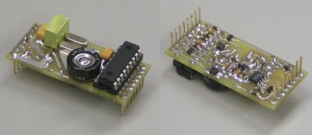
Talking about master clocks, the new multi-rate tracker / master clock prototype module is ready, worked first time. I attached a photograph.
The green part is a sub-miniature relay that toggles between both crystals (11.2896 and 12.288 MHz), the relay gives best performance, the electronic switches I tried increased jitter. The 100,000uF supercap in the center is required, without it, performance drops significantly. The 18-pin chip on the right is the "brains" of the multirate tracker. The required firmware was written by my brother, to give you an idea of his programming skills, he managed to modify the old tracker program in less than a quarter of an hour. Here he said, when he handed me the programmed micro controller, it should work like this. With some disbelief I put the chip in the test circuit, and guess what, the program worked first time.
This is not a straight-forward program, the micro controller runs on the selected master clock in order to minimize interference / inter-modulation. It has to maintain accurate timing for precise frequency measurement, while changing it's own clock frequency through the 12-bit DAC and VCXO. The program has to take into account that the micro could run on 2.8224, 5.6448 MHz, 3.072 MHz, or 6.144 MHz clock frequency. While doing so it has to determine the source sampling speed, and calculate relative correction factor to maintain real-time tracking. The program has to remain stable while toggling between crystals or changing clock division factor.
The picture on the right shows why the component side had only few parts. The VCXO master clock is built around a WF10192 clock chip, and a dual varactor. The power to the crystal is limited. The oscillator produces a nice low jitter sine wave that's then divided to achieve required bit clock. The WF10192 has an integrated divider that provides :1, :2, :4, and :8. The division factor can be set using 2 pins.
The square 100uH chokes are used for power supply filtering.
The module requires a reference clock (256fs) from the SPDIF receiver that runs in slave-clock mode. The module drives a "locked" LED indicating successful lock to applied sampling rate.
There are 3 sub-power supplies, one for the micro, one for the VCXO master clock, and one for the clock buffer. This way, crosstalk between these power supplies can be minimized. Screening will be added later, in order to reduce sensitivity to EM interference.
As you can see, I managed to put this tracker on the same module size as the single frequency tracker.
Yes, when using a balanced DAC (2 x TDA1543), and dual trans-impedance I/V converter / buffer for each channel. These could drive a bridge unity-gain power buffer. This way the output voltage, required at each trans-impedance converter could be halved.
Piggy-back clock buffers?
I wish it was that easy, clock buffers increase master clock jitter, the more cascaded buffers the worse this will get. Similar, connecting too many loads (clock buffers) to the master clock gives problems too. Clock buffers have a certain capacitance between both input and output, and there is always (on-chip) ground bounce, meaning that interference can travel both ways.
I currently use following bit clock distribution scheme:
Master clock > bit clock attenuator (330, 330, 100 Ohm) > TDA1543, shortest possible bit clock path.
Master clock > 390 Ohms > UHS buffer > 1K > load.
I now use 3.3V power supply for the TDA1543, so the 5Vpp bit clock needs to be attenuated. Without attenuation, the bit clock will attempt to "lift" TDA1543 3.3V power supply, resulting in increased interference.
The "dirty" loads are connected to the clock buffer using relatively high 1K series resistors, this reduces the power of the interference signals flowing back to the master clock output. I used 390 Ohm series resistor between master clock and buffer for similar reason.
Talking about master clocks, the new multi-rate tracker / master clock prototype module is ready, worked first time. I attached a photograph.
The green part is a sub-miniature relay that toggles between both crystals (11.2896 and 12.288 MHz), the relay gives best performance, the electronic switches I tried increased jitter. The 100,000uF supercap in the center is required, without it, performance drops significantly. The 18-pin chip on the right is the "brains" of the multirate tracker. The required firmware was written by my brother, to give you an idea of his programming skills, he managed to modify the old tracker program in less than a quarter of an hour. Here he said, when he handed me the programmed micro controller, it should work like this. With some disbelief I put the chip in the test circuit, and guess what, the program worked first time.
This is not a straight-forward program, the micro controller runs on the selected master clock in order to minimize interference / inter-modulation. It has to maintain accurate timing for precise frequency measurement, while changing it's own clock frequency through the 12-bit DAC and VCXO. The program has to take into account that the micro could run on 2.8224, 5.6448 MHz, 3.072 MHz, or 6.144 MHz clock frequency. While doing so it has to determine the source sampling speed, and calculate relative correction factor to maintain real-time tracking. The program has to remain stable while toggling between crystals or changing clock division factor.
The picture on the right shows why the component side had only few parts. The VCXO master clock is built around a WF10192 clock chip, and a dual varactor. The power to the crystal is limited. The oscillator produces a nice low jitter sine wave that's then divided to achieve required bit clock. The WF10192 has an integrated divider that provides :1, :2, :4, and :8. The division factor can be set using 2 pins.
The square 100uH chokes are used for power supply filtering.
The module requires a reference clock (256fs) from the SPDIF receiver that runs in slave-clock mode. The module drives a "locked" LED indicating successful lock to applied sampling rate.
There are 3 sub-power supplies, one for the micro, one for the VCXO master clock, and one for the clock buffer. This way, crosstalk between these power supplies can be minimized. Screening will be added later, in order to reduce sensitivity to EM interference.
As you can see, I managed to put this tracker on the same module size as the single frequency tracker.
Following with the variable I/V resistor DAC/Amp (you have to give it a good name, to chat about it), if I use the DI4M I will end with a balanced amp, which is very appealing ...or am I wrong?
Yes, when using a balanced DAC (2 x TDA1543), and dual trans-impedance I/V converter / buffer for each channel. These could drive a bridge unity-gain power buffer. This way the output voltage, required at each trans-impedance converter could be halved.
Attachments
Hi ecdesigns,
I am sure you and your brother share most of the genes 😀
That new super/duper multitracker clock, etc...sounds great but will you be selling separate modules?
(-cause I don-t think I can beat it myself 😀 )
For a balanced current buffer I found The Circlotron, or floating bridge amp.
http://www.passdiy.com/default.htm
Would it work?
Hey, I just finished modifying one of my active crossovers with charge transfer circuits and the benefits in terms of clarity and noise were evident even before the solder cooled down 😱
Many thanks for making my beloved Tannoy Autograph enclosures sound better.
Cheers,
M
Hi ECDesigns,
for the last few days, I have been searching thru the tDA1541a thread looking for the best analogue output of TDA1541A using IV stage and buffering.
I came across various design by Jocko, Guido (rather simplify) and others. When I read thru this thread, I found the IV stage as well which I think is huge improvement potential.
Since I am using single TDA 1541A (running in 4x with CS8412 and SAA7220), would you be kind enough to provide the IV stage and output (OPA627 + ECC82) ?
Hi Ecdesigns,
Your new DAC works on low power, right?
I know nothing about photoelectric cells, but have you thought about that possibility?
The other day I saw this programme about global warming where some inventor used acrylic Fresnel lens to direct concentrated light to increase a photoelectric cell-s efficiency ...😎
I assume that would be a low noise PS.
Cheers,
M
Hi Builder Brad,
When using 11.2896 MHz master clock, and DEM clock needs to be 352.8 KHz, the required division factor equals 11289600 / 352,800 = 32.
74HC4040 outputs:
Q0 (pin9), 5.6448 MHz, Q1 (pin7), 2.8224 MHz, , Q2 (pin6), 1.4112 MHz, Q3 (pin 5), 705.6 KHz, Q4 (pin 3), 352.8 KHz, Q5 (pin 2), 176.4 KHz, Q6 (pin 4), 88.2 KHz, Q7 (pin 13), 44,100 KHz, and so on. The last output Q11 (pin 1) outputs 2756.25 Hz.
So for 352.8 KHz DEM clock use pin 2, for 44.1 KHz WS signal use pin 13.
The 74HC4040 clock input (pin 10) goes to the 11.2896 MHz master clock, using 330 Ohm series resistor. Reset (pin 11) goes to GND.
The 74HC4040 is a ripple carry counter, meaning that the built-in flip-flops are triggered sequentially, this reduced ground-bounce. Ground bounce is a result of a sudden current surge (usually during simultaneous switching of multiple circuits), if there is no local decoupling cap that can supply required surge current (inside a chip), the supply voltage of the local circuit will drop as a result of this current surge, GND level will rise, VCC voltage level will drop. Ground-bounce effect increases with both supply voltage and switching frequency. Ground-bounce might lead to unwanted crosstalk, increased timing jitter, and even temporary circuit malfunction. The same effect can take place on a PCB with poor power supply decoupling.
I used a 74HC4040 in DI4MJ, DI4T and the new D1M DAC. It's either used to generate WS (DI4MJ / D1M) or both DEM clock and WS (DI4T).
I have a couple of spare 74HC040 chips - is there a schematic availible that uses these ICs for the diferential DEM reclock?
When using 11.2896 MHz master clock, and DEM clock needs to be 352.8 KHz, the required division factor equals 11289600 / 352,800 = 32.
74HC4040 outputs:
Q0 (pin9), 5.6448 MHz, Q1 (pin7), 2.8224 MHz, , Q2 (pin6), 1.4112 MHz, Q3 (pin 5), 705.6 KHz, Q4 (pin 3), 352.8 KHz, Q5 (pin 2), 176.4 KHz, Q6 (pin 4), 88.2 KHz, Q7 (pin 13), 44,100 KHz, and so on. The last output Q11 (pin 1) outputs 2756.25 Hz.
So for 352.8 KHz DEM clock use pin 2, for 44.1 KHz WS signal use pin 13.
The 74HC4040 clock input (pin 10) goes to the 11.2896 MHz master clock, using 330 Ohm series resistor. Reset (pin 11) goes to GND.
The 74HC4040 is a ripple carry counter, meaning that the built-in flip-flops are triggered sequentially, this reduced ground-bounce. Ground bounce is a result of a sudden current surge (usually during simultaneous switching of multiple circuits), if there is no local decoupling cap that can supply required surge current (inside a chip), the supply voltage of the local circuit will drop as a result of this current surge, GND level will rise, VCC voltage level will drop. Ground-bounce effect increases with both supply voltage and switching frequency. Ground-bounce might lead to unwanted crosstalk, increased timing jitter, and even temporary circuit malfunction. The same effect can take place on a PCB with poor power supply decoupling.
I used a 74HC4040 in DI4MJ, DI4T and the new D1M DAC. It's either used to generate WS (DI4MJ / D1M) or both DEM clock and WS (DI4T).
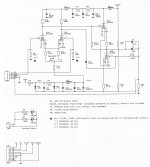
Hi ccschua,
I attached the differential-input tube amplifier schematics, used in the DI4T reference DAC. It uses 2 I/V passive resistors / channel (they are drawn in the schematic).
I personally wouldn't use (audio) Op-amps anymore, not even the best available today. The key issues are the required feedback loop, poor quality on-chip parts, and circuit complexity (difficult to predict and control circuit response). OP-amps rely on the feedback loop to keep distortion low. If the feedback loop fails (locks-out), distortion will increase rapidly, and might turn a 0.0005% THD OP-amp into a 10% THD OP-amp. The OP-amp connected to the DAC output will also be confronted with a very large bandwidth signal, so audio-OP-amps are likely to fail here.
The best I/V stage so far is the discrete trans-impedance converter, as it performs no active amplification. The DAC current isn't amplified, and the ac voltage is simply generated across an I/V resistor. All that's required now is buffering of the voltage across this I/V resistor.
Since I am using single TDA 1541A (running in 4x with CS8412 and SAA7220), would you be kind enough to provide the IV stage and output (OPA627 + ECC82) ?
I attached the differential-input tube amplifier schematics, used in the DI4T reference DAC. It uses 2 I/V passive resistors / channel (they are drawn in the schematic).
I personally wouldn't use (audio) Op-amps anymore, not even the best available today. The key issues are the required feedback loop, poor quality on-chip parts, and circuit complexity (difficult to predict and control circuit response). OP-amps rely on the feedback loop to keep distortion low. If the feedback loop fails (locks-out), distortion will increase rapidly, and might turn a 0.0005% THD OP-amp into a 10% THD OP-amp. The OP-amp connected to the DAC output will also be confronted with a very large bandwidth signal, so audio-OP-amps are likely to fail here.
The best I/V stage so far is the discrete trans-impedance converter, as it performs no active amplification. The DAC current isn't amplified, and the ac voltage is simply generated across an I/V resistor. All that's required now is buffering of the voltage across this I/V resistor.
Attachments
-ecdesigns- said:Hi Builder Brad,
When using 11.2896 MHz master clock, and DEM clock needs to be 352.8 KHz, the required division factor equals 11289600 / 352,800 = 32.
74HC4040 outputs:
Q0 (pin9), 5.6448 MHz, Q1 (pin7), 2.8224 MHz, , Q2 (pin6), 1.4112 MHz, Q3 (pin 5), 705.6 KHz, Q4 (pin 3), 352.8 KHz, Q5 (pin 2), 176.4 KHz, Q6 (pin 4), 88.2 KHz, Q7 (pin 13), 44,100 KHz, and so on. The last output Q11 (pin 1) outputs 2756.25 Hz.
So for 352.8 KHz DEM clock use pin 2, for 44.1 KHz WS signal use pin 13.
dear ecdesigns,
so in NOS mode (when bypassing SAA7220 in a cd player),and suppose we have a new 11.2896 Mhz dedicated Master Clock,
can we take WS (44.1khz) from pin 13 of the 74HC4040 instead of taking it from SAA7310 WSAB pin 4?
same with BCK+SCK (pin 2+4 on TDA1541A),can we take signal from Q1 (pin 7) of the 74HC4040 instead of taking signal from SAA7310 CLAB pin 3 ?
Thx.
Balanced DEM clock on DI8M
Attachted a solution for balanced dem clock on 352,8 kc
for the DI8M.
I tried a 74HC04. but the inverted chain has a time delay.
Audio not impressive.
Further I tried a 74HC86 for real balanced output.
It works but on the scope a lot of spikes and not a nice square wave. Audio did not impress me.
Then I tried a DS8921 and bingo : clean on the scope and a very noticable clean result on the audio. I like it.
Regards,
Onno
Attachments
-ecdesigns- said:Hi ccschua,
I attached the differential-input tube amplifier schematics, used in the DI4T reference DAC. It uses 2 I/V passive resistors / channel (they are drawn in the schematic).
I personally wouldn't use (audio) Op-amps anymore, not even the best available today. The key issues are the required feedback loop, poor quality on-chip parts, and circuit complexity (difficult to predict and control circuit response). OP-amps rely on the feedback loop to keep distortion low. If the feedback loop fails (locks-out), distortion will increase rapidly, and might turn a 0.0005% THD OP-amp into a 10% THD OP-amp. The OP-amp connected to the DAC output will also be confronted with a very large bandwidth signal, so audio-OP-amps are likely to fail here.
The best I/V stage so far is the discrete trans-impedance converter, as it performs no active amplification. The DAC current isn't amplified, and the ac voltage is simply generated across an I/V resistor. All that's required now is buffering of the voltage across this I/V resistor.
Pretty much effort, with a lot of potential disturbing sources.
From that perspective I'd rather stay with passive.
Below resistor on passive I/V output is for sure the best I tried.
http://www.rhopointcomponents.com/products.asp?recnumber=182
(I am aware that you're making your own Rs 😉 ) So I guess it all starts with the
selection of the right I/V-R. This is IMO one of the most important components of my
DAC. The gain of details in sound over e.g. Riken was pretty amazing.
However. I am looking for a battery ( +-6V) driven class-a (zero feedback) outputstage. I'd get along with 1,2 V-1,4V output voltage. I am wondering if anybody has built something like that?
Configurable balanced/unbalanced In/Out would be perfect.
I tried a Zapfilter II from LC-Audio. Pretty amazing how much more (transient-??) energy is delivered.
Especially on the low level details of percussion instruments and other pretty complex
instruments or on orchestral music I experienced quite a change. Though I am asking
myself if I can call this "neutral" reproduction ?? 😉 Anyhow. I'd like to give it a (DIY)-try.
THX
Cheers
Hi Soundcheck,
Ecdesigns' charge transfer power supply is comparable (I say it is better) to a battery PS, from his own words. The last differential amp he published for the DI4M (now apparently bettered by the D1M) has the other qualities you ask for...but it is optimized for the DI4M...
Hey John, if I understand well, your new D1M could work on a CD PRO trasnport, right? No need to design and build complex 48BCK timing chains 🙂
Personally, I am so pleased with my DI4M that I will build another one anyway...maybe two more (I have lots of TDA1543 😎 )
Cheers,
M
I am looking for a battery ( +-6V) driven class-a (zero feedback) outputstage.
Ecdesigns' charge transfer power supply is comparable (I say it is better) to a battery PS, from his own words. The last differential amp he published for the DI4M (now apparently bettered by the D1M) has the other qualities you ask for...but it is optimized for the DI4M...
Hey John, if I understand well, your new D1M could work on a CD PRO trasnport, right? No need to design and build complex 48BCK timing chains 🙂
Personally, I am so pleased with my DI4M that I will build another one anyway...maybe two more (I have lots of TDA1543 😎 )
Cheers,
M
maxlorenz said:Hi Soundcheck,
Ecdesigns' charge transfer power supply is comparable (I say it is better) to a battery PS, from his own words. The last differential amp he published for the DI4M (now apparently bettered by the D1M) has the other qualities you ask for...but it is optimized for the DI4M...
Hey John, if I understand well, your new D1M could work on a CD PRO trasnport, right? No need to design and build complex 48BCK timing chains 🙂
Personally, I am so pleased with my DI4M that I will build another one anyway...maybe two more (I have lots of TDA1543 😎 )
Cheers,
M
I am running everything on slightly buffered batteries. (My philosophy: "less is more").
It might be the case that the charge transfer is better then my high-end batteries.
I need to start at my current status quo though. I won't change my complete setup.
I'd be very happy to try a 12V charge transfer supply on my amp if it would be available to
me.
Don't forget - good shunts-regs will also perform better than Teddy-Regs I'd guess. You won't turn your entire system upside down because of this fact. The chase will never
end. Good - not to be a manufacturer. 😉
Anyhow: Has somebody posted/published anything related to class-a output stage earlier?
Cheers
Hi maxlorenz,
Yes I plan selling separate modules.
I already tested it, very low efficiency (average solar cell efficiency equals approx. 10%), and power supply ripple / hum is modulated on the LED output. Only advantage would be the galvanic insulation.
Some interesting links:
http://news.nationalgeographic.com/news/2007/02/070228-mars-warming.html
http://motls.blogspot.com/2004/09/sunspots-correlations-with-temperature.html
Yes, why not. It would halve the required ac output voltage at each trans-impedance converter.
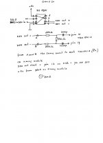
I attached some basic trans-impedance circuits that could be used for further experiments. The D1M is running on a highly optimized version, based on similar techniques. Note that the DAC current sink runs straight through T1 (that's kept in saturation), and directly flows through the passive I/V resistor R1. So basically iDAC = iRiv. I have to add that the 12V supply must be as clean as possible. The low-noise bandgap reference is required to provide approx. 2.1V DC at the TDA1543 output (2.7V - 0.6V).
The same circuit can be used for the TDA1541A, Vref now needs to be 0.6V (resulting at approx. 0V DC at TDA1541A output) . Simply use a silicon diode or a matched transistor connected as diode for replacing U1. TDA1541A has 4mA full-scale output current, so Riv needs to be lowered to 1K41 for achieving 2Vrms.
Yes, by leaving-out the timing-chain, the DAC will accept direct I2S from a CDPROII. But how do you plan to get the I2S signals transported to the DAC, without increasing bit clock jitter, and creating multiple (HF) ground loops? If you don't mind the (HF) ground loops, the CDPROII could even be slaved by the DAC, placing a low jitter clock in the DAC. But I doubt if the master clock remains a low jitter clock after the buffered master clock signal is fed back to the transport. The CDPROII will also output jitter on the I2S signals (even when using slave-clock mode). The jitter then simply enters the DAC through the I2S signals, and spreads all over the DAC electronics again.
The D1M now has a double SPDIF front-end, the first SPDIF receiver synchronously reclocks the incoming SPDIF signal using the recovered VCO MCK signal (SPDIF cleaner circuit). The cleaned-up SPDIF signal then enters the second, main SPDIF receiver (same type of SPDIF module). This receiver runs in slave-clock mode and provides a relatively clean MCK synchronization signal for the tracker.
That new super/duper multitracker clock, etc...sounds great but will you be selling separate modules?
Yes I plan selling separate modules.
Your new DAC works on low power, right?
I know nothing about photoelectric cells, but have you thought about that possibility?
I already tested it, very low efficiency (average solar cell efficiency equals approx. 10%), and power supply ripple / hum is modulated on the LED output. Only advantage would be the galvanic insulation.
The other day I saw this programme about global warming
Some interesting links:
http://news.nationalgeographic.com/news/2007/02/070228-mars-warming.html
http://motls.blogspot.com/2004/09/sunspots-correlations-with-temperature.html
For a balanced current buffer I found The Circlotron, or floating bridge amp. Would it work?
Yes, why not. It would halve the required ac output voltage at each trans-impedance converter.
The last differential amp he published for the DI4M (now apparently bettered by the D1M) has the other qualities you ask for...but it is optimized for the DI4M...
I attached some basic trans-impedance circuits that could be used for further experiments. The D1M is running on a highly optimized version, based on similar techniques. Note that the DAC current sink runs straight through T1 (that's kept in saturation), and directly flows through the passive I/V resistor R1. So basically iDAC = iRiv. I have to add that the 12V supply must be as clean as possible. The low-noise bandgap reference is required to provide approx. 2.1V DC at the TDA1543 output (2.7V - 0.6V).
The same circuit can be used for the TDA1541A, Vref now needs to be 0.6V (resulting at approx. 0V DC at TDA1541A output) . Simply use a silicon diode or a matched transistor connected as diode for replacing U1. TDA1541A has 4mA full-scale output current, so Riv needs to be lowered to 1K41 for achieving 2Vrms.
Hey John, if I understand well, your new D1M could work on a CD PRO transport, right? No need to design and build complex 48BCK timing chains
Yes, by leaving-out the timing-chain, the DAC will accept direct I2S from a CDPROII. But how do you plan to get the I2S signals transported to the DAC, without increasing bit clock jitter, and creating multiple (HF) ground loops? If you don't mind the (HF) ground loops, the CDPROII could even be slaved by the DAC, placing a low jitter clock in the DAC. But I doubt if the master clock remains a low jitter clock after the buffered master clock signal is fed back to the transport. The CDPROII will also output jitter on the I2S signals (even when using slave-clock mode). The jitter then simply enters the DAC through the I2S signals, and spreads all over the DAC electronics again.
The D1M now has a double SPDIF front-end, the first SPDIF receiver synchronously reclocks the incoming SPDIF signal using the recovered VCO MCK signal (SPDIF cleaner circuit). The cleaned-up SPDIF signal then enters the second, main SPDIF receiver (same type of SPDIF module). This receiver runs in slave-clock mode and provides a relatively clean MCK synchronization signal for the tracker.
Attachments

- Home
- Source & Line
- Digital Line Level
- Building the ultimate NOS DAC using TDA1541A