Hi Rembulan,
Thanks for your reply [post#1318]
You can find my website in my profile (homepage), just click on -ecdesigns- above my avatar.
I think it wouldn't be a problem to send a kit to Indonesia.
Thanks for your reply [post#1318]
You can find my website in my profile (homepage), just click on -ecdesigns- above my avatar.
I think it wouldn't be a problem to send a kit to Indonesia.
Hi taccodude,
Thanks for your reply [post#1319]
I have send you an email about this problem yesterday.
The pdf file is generated online, based on selections made. It could be possible that the latest pdf readers refuse to open it.
Please email the generated pdf file to me, and specify what type of operating system, browser and pdf reader you are using.
Reclocking frequency
Ecdesign,
I reread this thread and have a couple questions:
[1] Do the timing chains of both the DI8 and DI16 accept the both the 48BCK/frame and the 64BCK/frame, or just the 64BCK? The reason I ask is that a schematic with an "universal" timing chain module was posted.
[2] What clock frequency can be inputed into the DI8 and DI16 timing chains?
You said that:
"The DEM clock frequency for the TDA1541A is specified at 150...250 KHz. So I divided BCK (2.8224 MHz) by 16 using a synchronous counter. Frequency is now 176.4 KHz, it's in sync with BCK and it is within specified Dynamic Element Matching clock frequency range. When using a 470pF capacitor connected to the TDA1541A's DEM clock oscillator, it will run at approx. 200KHz."
And
Your universal DI2S Interface is connected to the master clock of 16.9344 MHz
16.9344 MHZ is 6X of 2.8224 MHZ
Can I assume that the master clock can be any frequency as long as it is a multiple of 2.8224 MHZ?
For example, can I use a clock of 22.5792 MHZ (8X of 2.8224 MHZ)?
Hi agent.5
Thanks for your reply [post #1323],
> I have designed two different timing-chains:
- Philips format timing-chain (this one is now used in the DI DACs), it only accepts 64BCK/frame, driving it with 48BCK/frame or 32BCK/frame would still provide sound, but the interpolation wouldn't work correctly, as the interpolated samples would have the wrong timing.
- Auto-detecting timing-chain (only used in Octal D-I DAC prototype), it automatically detects both 48BCK/frame and 64BCK/frame. Then it adapts the timing-chain taps accordingly, however I included the 48BCK/frame in order to support the direct I2S output from my Sony CD changer (Sony format). In order to do so, I had to include glue logic that converts the Sony format to the Philips format. This is basically done by a 7 BCK WS delay and inverting WS. This glue logic is also enabled / disabled depending on the detected 48BCK/frame or 64BCK/frame.
Another problem (for the DI 8 only) is DEM clock frequency. With 2.8224 MHz it's 2.8224 / 16 = 176.4 KHz, using 48BCK/frame, BCK would be 2.1168 MHz, resulting in a 132.3 KHz DEM clock rate, this is lower than the specified 150...250 KHz. In order to get the DEM clock within range again, another division factor would be necessary, like BCK divide by 12 > 176.4 KHz. I choose this DEM clock rate to make sure each active divider switch position lasts exactly WS/4.
> Higher BCK clock rates for the DI DACs are possible (TDA1541A / TDA1543 specs). Both, timing-chain and BCK buffers use fast logic and should have no problems with higher BCK clock rates.
> The universal DI2S interface uses the transport's master clock for synchronous reclocking of BCK only. For synchronous reclocking, a frequency running in sync with BCK is needed, like a multiple frequency of BCK, if you are using 2.8224 MHz BCK clock, 22.5792 MHz (8 x 2.8224 MHz) will work fine. Note that with 48BCK/frame, BCK equals 2.1168 MHz, and with fs = 44.1 KHz (MCLK / 48), a multiple frequency of 2.1168 MHz is needed.
The master clock of my Sony CD changer is 16.9344 MHz, it's 8 times the BCK frequency (2.1168 MHz).
For the shiftregister reclocker, a multiple frequency of BCK is preferred as well. I used 48 MHz in the USB/DI2S module, another option is 56.448 MHz.
48 MHz / 2.8224 MHz > 17.006 * fs
56 MHz / 2.8224 MHz > 20 * fs
I/V blanced conversion for octal dac
Dear John,
Sorry if this is a bit off the current subject but I am a newbee!!
I was thinking of useing your op amp I/V solution (blanced one) for one of my dac as no cap in the o/p seem a good idear. did you ever publish a pcb layout for the opamp i/v solution?- i did not see one (however i may have missed it!!- i have seen the circuit diagram)
Are we (the less electronicly gifted) 😕 privvy to see the PCB?--thanks for all your hard work so far.
Johnny555
PS are you soon to open a thread on the sonic resonators you have, that also seem very novel.
Hi Johnny555,
Thanks for your reply [post #1325]
> I have posted a schematic diagram of the I/V diff amp module, I could post the final version as well. Don't forget you need either 2 DAC chips, or a DAC chip with balanced outputs. The small I/V diff amp PCB (PCB-only) is available soon, it has all SMD decoupling caps pre-assembled. The module holds one channel only.
All DI DAC PCBs (PCB-only) can also be ordered separately, for modding / experimenting.
> First I need to complete the DI DAC project, the MOSFET cascode Power amplifier monoblocks and the Control amplifier. Next I will start a thread about the sonic resonators, I also plan to start a thread about manufacturing Printed Circuit boards.
thank you john
Thanks for the quick reply, i shall keep my eyes peeled for the PCB and sonic resonatore threads.
Johnny555
Thanks for the quick reply, i shall keep my eyes peeled for the PCB and sonic resonatore threads.
Johnny555
Price of DAC PCBS
John,
How much is a PCB that holds 4 TDA 1541 (ie your origional quad dac) and a timeing PCB (I assume its the normal Octal DAC PCB-unless its not?)
regards
Johnny555
John,
How much is a PCB that holds 4 TDA 1541 (ie your origional quad dac) and a timeing PCB (I assume its the normal Octal DAC PCB-unless its not?)
regards
Johnny555
Hi johnny555,
Thanks for your reply [post #1328]
The new DA1541A PCB holds only a single TDA1541A, this is done for easy "module swapping". This enables fine-tuning the DI 8(M), DAC modules can be swapped from the inverting to non-inverting group, in order to get lowest possible distortion, and matching both L + R channels as best as possible. Separate modules are also very handy during testing / trouble shooting.
The new DA1541A modules have both DATA and WS inputs voltage and bandlimited, reducing crosstalk to extreme low levels. Crosstalk from the DATA signal is significantly reduced, it's almost inaudible, but sow sound is very relaxing, and one can listen for many hours at relative high volume setttings without the slightest listening fatigue.
The sound is very smooth, but still contains all details, and response is very fast. BCK is fed to the DAC chip with a 22 Ohm resistor, higher series resistor values for BCK significantly increase both jitter and phase noise.
The DI8TIMP PCB holds the Philips format timing circuit, unlike the Octal DI DAC prototype that supports both Philips and Sony format. The DI8TIMP module is much more compact and uses less ICs.
I also done some tests with passive volume controls between DI 8M and the power amplifier. Seemed the DI 8M still had a big surprize in store, looked like the specified 0.0008 THD of the digital volume control chip, I used in my control amplifier was still way too high for my set. By replacing the control amplifier with a passive volume control, it became clear I was only listening to a fraction of the DI 8M performance (non-linear distortion of the cmos switches used in the volume control chip).
New Dac PCB
John,
Thank you for that, the new seperate DAC arrangement sounds better, what price is Each DAC board, and Mother board (which i assume they need to sit on) and the cost of the timeing PCB as i am poor and have to build it slowly
thanks John, keep us posted about the sonic resonators and the Amps, sounds like there could be some synergy in this system?.
regards
Johnny555
Anyone made a Bill of material for the DI-16 for North American suppliers like Mouser and Digikey ? I started mine but there are a lot of parts I can't source.
Hi John
Is it possible to switch with a chip the three I2S signals out of a SAA 7210, and then best solution regarding sound quality (jitter?)
I want to add a USB entrance on my CDP and keep I2S, to switch between USB audio from PC and the CDP itself. For USB to I2S want to use PCM2706/7
Thanks.
Is it possible to switch with a chip the three I2S signals out of a SAA 7210, and then best solution regarding sound quality (jitter?)
I want to add a USB entrance on my CDP and keep I2S, to switch between USB audio from PC and the CDP itself. For USB to I2S want to use PCM2706/7
Thanks.
USB / large bandwidth signal processing
Hi Tubee,
Thanks for your reply [post #1332]
I used the DS8921 / DS8922 both as buffer and as switch (the DS8922 has separate enable inputs). The DS8922 outputs are connected in parallel, and the chip that buffers the desired input is enabled, the other one remains in tri-state. You could also use the USB/DI2S module (PCB) from the DI DACs, it already has the I2S switching function, contains a USB receiver chip and the shiftregister reclocker, that is absolutely necessary to get high-end sound quality from the USB receiver chip. The direct output from the PCM2706 / PCM2707 is far worse than SPDIF (jitter). I posted oscillograms illustrating this fact on this thread.
In addition to low jitter, I recently discovered that pre-amplifier, interlinks, power amplifier and speaker crossover filter need to respond lightning fast (bandwidth 1 MHz or higher). Even the best coupling / speaker crossover filter caps seem to be way to slow. The reason for this is to avoid introducing additional HF inter-modulation distortion in power amplifier and speaker crossover filter, it also provides fastest possible signal response times.
This way, the (NOS) DAC output signal is processed as a plain wide bandwidth signal all the way up to the tweeter terminals (the presence of HF signals now becomes more or less irrelevant). In other words, I adapted my set to handle HF signals. Then, due to the mechanical limitations of the tweeter, it will act as a acoustic filter. I have obtained staggering results with this technique using the DI 8M. The increase in sound quality exceeds all modifications made to the DI DACs by far, it's noticed immediately. Sound is now super smooth, while preserving full detail and micro-information.
Both DAC groups and I/V converters have been modified / fine-tuned to get exceptional low level performance. The tube diff-amp is also modified (much faster and lower output impedance). One of the reasons for the wonderful sound of the mixed-mode output is the fact that tubes have no thermal memory like semiconductors have. Since half of the signal is being processed by the tube output stage, distortion caused by thermal memory is significantly reduced.
Hi John
Thanks for elaboration of USB-I2S and switch. Have an DS8922 at hand, had to order two that time, one ended up in CD304 as Spdif transmitter (but never used it though!)
My ex boss gave me a old slow Compaq E500 900Mhz coppermine laptop, this one is nice silent as music server. Have ordered more ram, and repaired the broken off USB jack on mainboard. Made it dual boot with Linux Kubuntu and win 2k. And you may guess John wich OS is giving install problems....
Also Doede Douma uses the PCM2707 as USB-I2S converter, but doesn't reclock I2S in his implementation.
I reclocked 2.8 mHz Bcl only on my experimental PCM56 setup (two cascaded 74/00 dual input Nand's) it sounded very slighly better. For serial to parallel conversion of data and to fit I2S to PCM's input format i used a universal circuit, but i have a slight suggestion a 3 chip thus simpler circuit, (with timing error, R dac gets its data half WS cycle later) sounded some better. The TDA1541 also has this timing error, because it has a single serial digital input and is a stereo dac.
The MSB adjust is very important for the PCM. The 1541 has 4mA offset on output (a "single ended" output?), the PCM56 not, thats problably why the MSB adjust is important. But i am not a specialist on this.
After the PCM56 i use Pedja's AD844 I/V, a very fast opamp used as a grounded base amp. Sounds quite good, indeed very fast. But have parts home to build a tube I/V.
I also believe in the fact that the rest of the audio chain must be capable of some HF. That's why i listen now to allmost all tube gear, except the the powertransistors, they are FET's. Have build several amps, the hybrid sounded best. But fortunately these days its becoming better, there are more good opamps (LM4562) seeing daylight, maybe they sound so good because of higher bandwith.
Thanks for elaboration of USB-I2S and switch. Have an DS8922 at hand, had to order two that time, one ended up in CD304 as Spdif transmitter (but never used it though!)
My ex boss gave me a old slow Compaq E500 900Mhz coppermine laptop, this one is nice silent as music server. Have ordered more ram, and repaired the broken off USB jack on mainboard. Made it dual boot with Linux Kubuntu and win 2k. And you may guess John wich OS is giving install problems....
Also Doede Douma uses the PCM2707 as USB-I2S converter, but doesn't reclock I2S in his implementation.
I reclocked 2.8 mHz Bcl only on my experimental PCM56 setup (two cascaded 74/00 dual input Nand's) it sounded very slighly better. For serial to parallel conversion of data and to fit I2S to PCM's input format i used a universal circuit, but i have a slight suggestion a 3 chip thus simpler circuit, (with timing error, R dac gets its data half WS cycle later) sounded some better. The TDA1541 also has this timing error, because it has a single serial digital input and is a stereo dac.
The MSB adjust is very important for the PCM. The 1541 has 4mA offset on output (a "single ended" output?), the PCM56 not, thats problably why the MSB adjust is important. But i am not a specialist on this.
After the PCM56 i use Pedja's AD844 I/V, a very fast opamp used as a grounded base amp. Sounds quite good, indeed very fast. But have parts home to build a tube I/V.
In addition to low jitter, I recently discovered that pre-amplifier, interlinks, power amplifier and speaker crossover filter need to respond lightning fast
I also believe in the fact that the rest of the audio chain must be capable of some HF. That's why i listen now to allmost all tube gear, except the the powertransistors, they are FET's. Have build several amps, the hybrid sounded best. But fortunately these days its becoming better, there are more good opamps (LM4562) seeing daylight, maybe they sound so good because of higher bandwith.
This way, the (NOS) DAC output signal is processed as a plain wide bandwidth signal all the way up to the tweeter terminals (the presence of HF signals now becomes more or less irrelevant). In other words, I adapted my set to handle HF signals.
I remember articles in the discontinued magazine Audio & Techniek, that bypassing of tweeter Xover cap with a very small KS or styrene cap does improve sound. Value around 10N allready sufficient.

tubee said:The TDA1541 also has this timing error, because it has a single serial digital input and is a stereo dac.
.
There are many things wrong with the TDA1541 but that is not one of them.
Does anyone have a comment as to why the TDA1641A seems to be so popular? Is it a fad? Aren't there newer DACs that do a better job? Any comments?
TDA1541A
Hi gjash,
Thanks for your reply [post #1338]
The TDA1541A uses a unique DEM Dynamic Element Matching technique (patented by Philips). This technique continuously "calibrates" the 6 most significant bits of the DAC at a rate of approx. 50,000 times a second (200 KHz / 4). It averages the input current, and divides it in 4 exactly equal currents. This way component tolerances and chip aging are constantly corrected. All binary weighted currents (D0...D15) are derived from one single reference source. This DEM circuitry used, is also the reason why the TDA1541A needs the 14 decoupling caps (7 for each channel) unlike all other DAC chips.
The TDA1541A doesn't use switched resistive ladder networks, but pure constant current sources. It uses very low voltages (few hundred milivolts) to control the digital functions, this greatly reduces crosstalk. The fast current driven logic eliminates glitches at the DAC output, providing a very "clean" signal.
The analog circuitry provides good sonic properties (each DAC chip, like OP-amps has a specific sonic "fingerprint". So despite superior specifications, perceived sound quality can still be very disappointing due to various DAC parameters, Similar like with OP-amps. Modern delta sigma converters use HF switching techniques, my personal experience with these is that there is "something" present in the sound that prevents relaxed listening. With the TDA1541A, the sound is smooth warm and natural, one is "drawn" into the music right from the start and can listen for many hours without listening fatigue.
Something often forgotten is thermal memory, a DAC chip, can have superior specs, but they tell little about non-linear distortion caused by thermal memory effects. That's why tubes can sound so natural and transparent despite their relatively high distortion figures, as they have no thermal memory. It seems that the designers of the TDA1541A did something that resulted in lower sensitivity to the effects of thermal memory, when this is true, it could be the reason that the TDA1541A can still outperform DAC chip with superior specs, suffering from thermal memory effects.
The TDA1541A is used in various High-end DACs and CD players, just check the internet. If it was a bad sounding chip, nobody would use it for these kind of applications. Often a single TDA1541A is used, and TDA1541A performance is almost always based on the performance of a single chip, but when multiple TDA1541A chips are used, like the 8 in the DI8M, extreme results are possible. But it's not the DAC chip alone, the analog circuit that follows it is even more important.
Another advantage of the TDA1541A is that it's a separate DAC chip that can be easily interfaced. Because it's a separate chip, the surrounding electronics can be optimized for best performance. It can also be used in NOS mode. Modern DAC chips have everything integrated, if they sound bad, there is little one can do to improve this.
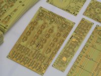
Ecdesigns,
Does your PCB is handmade or is a company that make it for you ?
Can you tell wich ?
It looks so nice !... 🙂
Does your PCB is handmade or is a company that make it for you ?
Can you tell wich ?
It looks so nice !... 🙂
- Home
- Source & Line
- Digital Line Level
- Building the ultimate NOS DAC using TDA1541A