DI8 configuration
DI8
The attached drawing illustrates the DI8 configuration. On the top left is the DI8 main power supply, it can be wired for both 115 and 230V. It drives logic circuitry and the DI8 core. Remote power on/off function can be added if desired.
Next is the USB/DI2S interface, it provides both USB and differential I2S inputs. The USB circuitry includes a shiftregister reclocker, the DI2S goes straight to the DAC chips. The module automatically toggles between USB and DI2S, USB has highest priority. There are outputs provided to drive a two color indication LED.
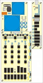
At the top right is the DI8 core, it consists of the DI8 mainboard, and a number of modules mounted on top of it. The DI8 mainboard holds all interconnections, filters for each power supply connection, DEM clock filter / attennuator and DEM clock coupling caps. The following modules are mounted on top of the DI8 mainboard: DI8 timing module, 8 x DAC module and 2 X I/V diff amplifier module.
DI8
The attached drawing illustrates the DI8 configuration. On the top left is the DI8 main power supply, it can be wired for both 115 and 230V. It drives logic circuitry and the DI8 core. Remote power on/off function can be added if desired.
Next is the USB/DI2S interface, it provides both USB and differential I2S inputs. The USB circuitry includes a shiftregister reclocker, the DI2S goes straight to the DAC chips. The module automatically toggles between USB and DI2S, USB has highest priority. There are outputs provided to drive a two color indication LED.
At the top right is the DI8 core, it consists of the DI8 mainboard, and a number of modules mounted on top of it. The DI8 mainboard holds all interconnections, filters for each power supply connection, DEM clock filter / attennuator and DEM clock coupling caps. The following modules are mounted on top of the DI8 mainboard: DI8 timing module, 8 x DAC module and 2 X I/V diff amplifier module.
Attachments

DI16 configuration
DI16
The attached drawing illustrates the DI16 configuration. At the top left is the DI16 main power supply, it can be wired for both 115 and 230V. It drives logic circuitry and the DI16 core. Remote power on/off function can be added if desired.
At the top right is the USB/DI2S interface, it provides both USB and differential I2S inputs. The USB circuitry includes a shiftregister reclocker, the DI2S goes straight to the DAC chips. The module automatically toggles between USB and DI2S, USB has highest priority. There are outputs provided to drive a two color indication LED.
At the bottom is the DI16 core, it contains 16 X TDA1543, DI16 timing and I/V diff amp.
Attachments
DI16M configuration
DI16M
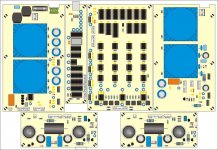
The attached drawing illustrates the DI16M configuration. On the top left is the DI8 main power supply, it can be wired for both 115 and 230V. It drives logic circuitry and the DI16 core. Remote power on/off function can be added if desired.
Next is the USB/DI2S interface, it provides both USB and differential I2S inputs. The USB circuitry includes a shiftregister reclocker, the DI2S goes straight to the DAC chips. The module automatically toggles between USB and DI2S, USB has highest priority. There are outputs provided to drive a two color indication LED.
In the center is the DI16 core, it contains 16 X TDA1543, DI16 timing and I/V diff amp.
On the top right is the tube power supply, it can be wired for both 115 and 230V. It drives both tube diff amp modules (filament voltage + high voltage). It has a integrated soft start circuitry for the filaments and a delayed power-on for the high voltage.
At the bottom are the two tube diff amp modules, necessary for the "mixed" mode. They consist of a differential amplifier (ECC83S balanced) and a cathode follower (ECC81).
DI16M
The attached drawing illustrates the DI16M configuration. On the top left is the DI8 main power supply, it can be wired for both 115 and 230V. It drives logic circuitry and the DI16 core. Remote power on/off function can be added if desired.
Next is the USB/DI2S interface, it provides both USB and differential I2S inputs. The USB circuitry includes a shiftregister reclocker, the DI2S goes straight to the DAC chips. The module automatically toggles between USB and DI2S, USB has highest priority. There are outputs provided to drive a two color indication LED.
In the center is the DI16 core, it contains 16 X TDA1543, DI16 timing and I/V diff amp.
On the top right is the tube power supply, it can be wired for both 115 and 230V. It drives both tube diff amp modules (filament voltage + high voltage). It has a integrated soft start circuitry for the filaments and a delayed power-on for the high voltage.
At the bottom are the two tube diff amp modules, necessary for the "mixed" mode. They consist of a differential amplifier (ECC83S balanced) and a cathode follower (ECC81).
Attachments
Hello EC,
Will one be able to purchase the tube PCBs at a later stage?
In other words, can one opt for a LM4562-only version and 'upgrade' later?
Thanks! 🙂
Will one be able to purchase the tube PCBs at a later stage?
In other words, can one opt for a LM4562-only version and 'upgrade' later?
Thanks! 🙂
Great!
Please consider a kit (or the schematics) to make the DI2S circuit at the transport.
(of course, there's always this little compatibility problem with the CD PRO transport remaining... )
)
Bye,
M
Please consider a kit (or the schematics) to make the DI2S circuit at the transport.
(of course, there's always this little compatibility problem with the CD PRO transport remaining...
)Bye,
M
Hi adhoc,
Thanks for your reply [post#1284]
Yes, of course it's possible to order PCBs separately, so it's no problem to add the tube (mixed mode) option later.
Thanks for your reply [post#1284]
Yes, of course it's possible to order PCBs separately, so it's no problem to add the tube (mixed mode) option later.
DI2S interface schematics
Hi maxlorenz,
Thanks for your reply [post #1285]
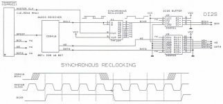
Here is a diagram of a simple interface circuit that enables connecting digital sound sources to the DI DACs. I am using the same circuit, but with a CS8412 to connect my Sony CD changer to the DI 8 and DI 16. It provides a lower jitter bit clock than the I2S bit clock derived directly from the LSI chip.
This circuit is part of the universal I2S interface, the interface also has a by-passable shiftregister reclocker. This reclocker can be used with digital sound sources that haven't got a master clock output available.
Hi maxlorenz,
Thanks for your reply [post #1285]
Here is a diagram of a simple interface circuit that enables connecting digital sound sources to the DI DACs. I am using the same circuit, but with a CS8412 to connect my Sony CD changer to the DI 8 and DI 16. It provides a lower jitter bit clock than the I2S bit clock derived directly from the LSI chip.
This circuit is part of the universal I2S interface, the interface also has a by-passable shiftregister reclocker. This reclocker can be used with digital sound sources that haven't got a master clock output available.
Attachments
Thanks, EC.
It seems that USB is the easiest way to go with your DACs.
I would rather try to go direct I2S to DI2S, using the final part of the circuit, instead of using the SPDIF out...or find a Philips format I2S transport...🙁 for direct connection.
Bye,
M
It seems that USB is the easiest way to go with your DACs.
I would rather try to go direct I2S to DI2S, using the final part of the circuit, instead of using the SPDIF out...or find a Philips format I2S transport...🙁 for direct connection.
Bye,
M
The tda1541a datasheet shows a 100nf cap between pin 5 /14 to pin 28 and 100nf cap between pin 15 and 26.
I can't see how you can get the digital ground decoupled properly...
I can't see how you can get the digital ground decoupled properly...
DI8 grounding / noise reduction
Hi ash_dac,
Thanks for your reply [post #1289]
The TDA1541A has a separate analog (pin5) and digital (pin14) ground connection.
When connecting both together, close to the chip, the return path for the digital signals will take the route of the lowest (HF) resistance. If this is analog ground, it will travel along analog ground, and super-imposes on the analog signal.
In the DI8, a large analog ground plane is used as reference for the analog signals. All DAC modules, I/V diff modules and tube diff amp modules are connected to this analog ground plane.
The DI8 DA module has a separate digital ground connection. All DA modules are connected to this digital ground (pin14). The timing-chain and I2S input signals are referenced to this digital ground. Each DAC module, even the I/V diff modules have on-board voltage regulators with very short connections to the chip(s). All power supply voltages (+5V, -5V, +15V and -15V are thoroughly decoupled to the analog ground by using audio grade Panasonic electrolytic capacitors in parallel with ceramic SMD caps. The value for the electrolytic capacitors is chosen as high as possible for the available space (33...100uF). The HF return path is kept very short as each module power supply input is filtered by a separate Murata filter (28 for the analog power supply lines).
Both analog and digital ground are interconnected on the DI8 mainboard by using the ferrite beads of a Murata filter. This imposes a short circuit for DC and a relatively high resistance for HF signals. This way the digital ground has the lowest resistance for HF signals, and these are then forced to take this route, isolating them from the analog signals.
The power supplies are star grounded to analog ground.
In order to reduce noise, hum and interference even further, I use pre-regulators in the DI8. So the analog power supplies are stabilized twice. Both DATA and WS input voltage of each DAC module are now limited to 3.3V (exept BCK to maintain very low jitter). This way the digital switching noise amplitude is limited. Same applies for the DEM clock, it's amplitude is limited by a attenuator and higher harmonics are filtered in order to reduce noise levels. A ring core transformer is used to enable injecting the DEM clock while maintaining HF separation between both analog and digital ground (DEM clock is referenced to analog ground).
Soft recovery and Skottky barrier diodes are used in the power supplies to minimize switching noise.
The TDA1541A temperature is kept relatively low (around 45...50 degrees Celcius) by using a large heatsink, lower temperatures means lower noise. Due to the thermal coupling between the DAc chips, temperature drift is minimized. The dissipation varies between TDA1541A chips. The dissipation is not caused by errors in power supplies, DI setup, paralleling TDA1541A current outputs, or using a external DEM clock. I already checked that.
The heatsink also acts like a screen that attenuates some HF radiation, lowering it's effect on the analog circuitry.
The DI DACs use a streamlined signal flow. The digital I2S and clock signals enter one side of the PCB, first comes the timing chain (digital), next the DAC modules (digital > analog), then at the other side of the PCB the actual analog signal is generated, far away from the digital signals on the other side of the PCB. I kept the digital connections very short, that's why I put the digital section close to the rear of the housing. By doing so, I avoid unnecessary crosstalk (HF signals induce crosstalk much more easily than LF signals) and obtain lowest jitter. The analog signal leaves the PCB at the front side of the housing, it still has a massive combined 55Vpp amplitude that won't pick-up noise easily. It is routed to the back of the housing trough a high-quality screened cable, that runs trough a aluminum cable duct (double screening). The attenuator soldered directly to the RCA sockets, reduces the analog output signals to 1V rms (2V rms in my set), and also attenuates (picked-up) noise / interference effectively.
The tube amplifier uses a soft-start stabilized filament supply, and a quad stabilized HV supply (pre regulator + 2 cascaded zener diodes + a post regulator for each separate triode). The tube diff amp has a high CMMR and very low distortion, it is driven by a accurate current source. The current source negative supply voltage has double stabilizing (2 cascaded zener diodes). Hum is almost non-existent. By using the mixed mode, noise generated by the tube amplifier is averaged with the OP-amp diff amplifier, resulting in very low noise levels, much lower than that of tubes only.
The measures taken to reduce noise / crosstalk , resulted in exceptional low noise, even without using a analog filter!
-ecdesigns-
2) DI8M (DI8 with mixed mode outputs, tube + LM4562), 17PCBs
- 1 X DI8 mainboard + DEM clock ringcore transformer
- 1 X DI8 timing module + pre-assembled SMD parts (capacitors + resistors + UHS buffers) + PALCE16V8
- 8 X DA converter module (TDA1541A) + pre-assembled SMD parts (capacitors + zener diodes)
- 2 X I/V diff module + pre-assembled SMD parts (capacitors)
- 1 X USB/DI2S module + pre assembled SMD parts (PCM2706 + capacitors + resistors + UHS logic)
- 1 X DI8 power supply module + pre-assembled SMD part (resistor)+ tube status LED controller
- 1 X Tube power supply module
- 2 X Tube diff amplifier module
I would like to order one of this kit,
what is the price paying through Paypal.
Re: DI8 grounding / noise reduction
(DAC) pins describe what they connected to on the inside, it does not say anything on how to connect them on the outside.
Standard practice with a dac is to connect agnd and dgnd straight at the dac. AD and BB are very clear on this (philips is not that good with info). AD has an appl note which describes why.
I would have a digital groundplane, so the noisy dig. signals have a returnpath close to the signal line. No interruptions with wires.
Actually the ground pins on the 1541 are not carrying a lot of current. Digital signals is mainly +5 and -5 and analog signals +5.
You're listening to your coupling caps with all those (pre)regulators.
You're listening to your coupling caps with all those (pre)regulators.
Hi Guido
Can you enlighten this?
Hi Mikewong,
Thanks for your order [post #1291]
I plan to carry out a major website update this weekend, then you can use the online product configurator to select the desired items. It will then automatically generate a PDF with pricing information, and a complete list of the items selected. The PDF can then be emailed to place an order.
Grounding issues / TDA1541A internal circuitry
Hi Guido,
Thanks for your tip [post #1292]
I agree, it would be nice to have some more detailed information about the TDA1541A internal circuitry to optimize decoupling / grounding. It know it's common practice to connect analog and digital ground close to the DAC, but I use 8 or 16 DACs. When I connect analog and digital ground together, close at each DAC chip, it basically means the analog ground plane is also used as return path for the digital signals (I2S, clock), and it will interfere with the analog signal return path.
I do have a large ground plane on the analog mainboard (where all modules are connected to). This is my analog reference ground. It has very low resistance and a mesh pattern. Electro Magnetic interference caused by currents running trough it, is kept away from the modules by the relatively large distance between ground plane and modules. With a multilayer board for instance, the EMI is directly injected to the components located very close to it.
The DI DACs are fully symmetrical, even the PCB lay-out. so common noise, picked-up by whatever source is effectively canceled at the differential output stage. Did I mention the differential stage test where I put a 2V! pp hum on the TDA1543 power supply (DI 16), 4 V DC plus 2Vpp hum! Well the DI 16 performed like there was nothing wrong with it.
All supply voltages have filters to prevent long loops for HF signals. In critical digital circuits like the clock and driver, every single chip is separately isolated from the power supply (series resistor) to keep HF path as short as possible.
All (local) voltage regulators are placed close to the DAC / OP-amp ground reference, so the supply voltage for these components won't pick up much interference, as would be the case if the voltage regulators were placed on the power supply board.
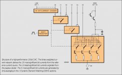
I have studied the TDA1541A internal architecture, basically it has one reference current source (4mA), tied to -15V. All 16, binary weighted currents are derived from this single reference current source. The bit switches compose the output current from these 16 binary weighted currents. Three 2-bit active dividers (DEM circuitry) split-up the currents of the reference source into 4 equal currents by means of resistors. DEM circuitry is used to average between these four divided currents, matching them as closely as possible. Same is done in the other two active dividers, they are connected to one of the previous active divider outputs. The DEM clock drives the four averaging switches in each active divider. They basically keep swapping between 4 current outputs with a specific pattern: 2,3,1,4 > 1,2,4,3 > 4,1,3,2 > 3,4,2,1 The 2 X 7 decoupling caps are connected between ground and the active divider outputs. If drift occurs, it will affect all output currents in the same way as they are derived from the same reference current source. Due to the DI 8 balanced design, even this is being compensated. If the active divider resistors age / drift, this will be compensated by the DEM circuitry. MSB tuning makes little sense here because the DEM circuitry automatically matches / averages the divided currents with a rate of approx. 150...250 KHz.
By synchronizing the DEM clock with BCK, the exact moment of driving the DEM switches coincides with BCK, preventing inter-modulation that occurs with a free running DEM clock. The DI 8 uses exactly 4 DEM cycles within one sample time (2822400 / 16 = 176.4 KHz, 176.4 / 44100 = 4).
The 10 LSBs are derived from a passive divider (emitter scaling), connected to one output of the third active divider. The output of the TDA1541A is a current sink to -15V. Due to the lack of more detailed information, I assume that both +5V and -5V are used to feed the digital circuits and level shifters. I have added a block diagram of the TDA1541A internal circuitry for reference.
I choose the Audio grade coupling caps because they cost about the same as standard caps, but have better (audio) specifications. I didn't use tantalium caps anymore because they are quite expensive (especially the higher values). The local voltage regulators effectively prevent crosstalk between chips as their power supplies are now isolated. They also protect every single module in case of a voltage surge or power supply malfunction. Since the TDA1541A output current accuracy is determined by a constant current source, tolerances in the local voltage regulators of each DAC module should have little or no effect.
Hi Guido,
Thanks for your tip [post #1292]
I agree, it would be nice to have some more detailed information about the TDA1541A internal circuitry to optimize decoupling / grounding. It know it's common practice to connect analog and digital ground close to the DAC, but I use 8 or 16 DACs. When I connect analog and digital ground together, close at each DAC chip, it basically means the analog ground plane is also used as return path for the digital signals (I2S, clock), and it will interfere with the analog signal return path.
I do have a large ground plane on the analog mainboard (where all modules are connected to). This is my analog reference ground. It has very low resistance and a mesh pattern. Electro Magnetic interference caused by currents running trough it, is kept away from the modules by the relatively large distance between ground plane and modules. With a multilayer board for instance, the EMI is directly injected to the components located very close to it.
The DI DACs are fully symmetrical, even the PCB lay-out. so common noise, picked-up by whatever source is effectively canceled at the differential output stage. Did I mention the differential stage test where I put a 2V! pp hum on the TDA1543 power supply (DI 16), 4 V DC plus 2Vpp hum! Well the DI 16 performed like there was nothing wrong with it.
All supply voltages have filters to prevent long loops for HF signals. In critical digital circuits like the clock and driver, every single chip is separately isolated from the power supply (series resistor) to keep HF path as short as possible.
All (local) voltage regulators are placed close to the DAC / OP-amp ground reference, so the supply voltage for these components won't pick up much interference, as would be the case if the voltage regulators were placed on the power supply board.
I have studied the TDA1541A internal architecture, basically it has one reference current source (4mA), tied to -15V. All 16, binary weighted currents are derived from this single reference current source. The bit switches compose the output current from these 16 binary weighted currents. Three 2-bit active dividers (DEM circuitry) split-up the currents of the reference source into 4 equal currents by means of resistors. DEM circuitry is used to average between these four divided currents, matching them as closely as possible. Same is done in the other two active dividers, they are connected to one of the previous active divider outputs. The DEM clock drives the four averaging switches in each active divider. They basically keep swapping between 4 current outputs with a specific pattern: 2,3,1,4 > 1,2,4,3 > 4,1,3,2 > 3,4,2,1 The 2 X 7 decoupling caps are connected between ground and the active divider outputs. If drift occurs, it will affect all output currents in the same way as they are derived from the same reference current source. Due to the DI 8 balanced design, even this is being compensated. If the active divider resistors age / drift, this will be compensated by the DEM circuitry. MSB tuning makes little sense here because the DEM circuitry automatically matches / averages the divided currents with a rate of approx. 150...250 KHz.
By synchronizing the DEM clock with BCK, the exact moment of driving the DEM switches coincides with BCK, preventing inter-modulation that occurs with a free running DEM clock. The DI 8 uses exactly 4 DEM cycles within one sample time (2822400 / 16 = 176.4 KHz, 176.4 / 44100 = 4).
The 10 LSBs are derived from a passive divider (emitter scaling), connected to one output of the third active divider. The output of the TDA1541A is a current sink to -15V. Due to the lack of more detailed information, I assume that both +5V and -5V are used to feed the digital circuits and level shifters. I have added a block diagram of the TDA1541A internal circuitry for reference.
I choose the Audio grade coupling caps because they cost about the same as standard caps, but have better (audio) specifications. I didn't use tantalium caps anymore because they are quite expensive (especially the higher values). The local voltage regulators effectively prevent crosstalk between chips as their power supplies are now isolated. They also protect every single module in case of a voltage surge or power supply malfunction. Since the TDA1541A output current accuracy is determined by a constant current source, tolerances in the local voltage regulators of each DAC module should have little or no effect.
Attachments
Re: Grounding issues / TDA1541A internal circuitry
The info on the internals 1541 is here on diyaudio, there's a search button.
current ref source is from -15 to -5.
i would also sync DEM with BCK, but NOT when BCK changes state (which latches the outputs)
offset current -2mA goes to -15 indeed, but analog audio current goes to +5. Now imagine how it flows through from i/v through coupling caps and series regs (if used).
+5 and -5 are indeed for digital stuff.
-ecdesigns- said:I agree, it would be nice to have some more detailed information about the TDA1541A internal circuitry to optimize decoupling / grounding.
I have studied the TDA1541A internal architecture, basically it has one reference current source (4mA), tied to -15V.
By synchronizing the DEM clock with BCK, the exact moment of driving the DEM switches coincides with BCK, preventing inter-modulation that occurs with a free running DEM clock.
the TDA1541A is a current sink to -15V.
I assume that both +5V and -5V are used to feed the digital circuits and level shifters.
The info on the internals 1541 is here on diyaudio, there's a search button.
current ref source is from -15 to -5.
i would also sync DEM with BCK, but NOT when BCK changes state (which latches the outputs)
offset current -2mA goes to -15 indeed, but analog audio current goes to +5. Now imagine how it flows through from i/v through coupling caps and series regs (if used).
+5 and -5 are indeed for digital stuff.
From the Saa7220 datasheet development data....
Grounds connected at chip I guess but I think there's a few errors.
-12V on VDD2!
-15V on VDD1
Not sure I'd try it!
An externally hosted image should be here but it was not working when we last tested it.
Grounds connected at chip I guess but I think there's a few errors.
-12V on VDD2!
-15V on VDD1
Not sure I'd try it!
Guido, I was once suggested to use a 7810 or equivalent grounded to the -15v line and powered from ground to get -5v, any reason?
I agree, it would be nice to have some more detailed information about the TDA1541A internal circuitry to optimize decoupling / grounding.
http://www.diyaudio.com/forums/showthread.php?postid=366490
- Home
- Source & Line
- Digital Line Level
- Building the ultimate NOS DAC using TDA1541A