this is the visual presentation of Sin(x)/x function, it is not as wroted slightly different:

.
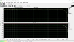
this is the graph of what should be happening in HF domain:

and Zanden propose among other citcuits this one:

.
the whole PDF for sin(x)/x is here:
.
I will send the PDF for calculating RLC values with chosen Q and corrected Q for every RLC branch.
.
this is the graph of what should be happening in HF domain:
and Zanden propose among other citcuits this one:
.
the whole PDF for sin(x)/x is here:
.
I will send the PDF for calculating RLC values with chosen Q and corrected Q for every RLC branch.
Attachments
No it just attenuate n x Fs points with chossen Q for each BW. That can be adjusted to inclode the images too. So additional passive circuit is welcome?The Zanden circuit realizes anti-sinc correction?
.
I saw Your solution for compensating basic Fs for NOS. I think that is good idea that working.
.
Thorsten has one passive circuit prior to ecc88 tube stage for dac, if I am remebering well?
.
https://pearl-hifi.com/06_Lit_Archive/14_Books_Tech_Papers/Loesch_Thorsten/Tube Stages for DACs.pdf
.
and
Hi:
I am planning to build TDA1541 based DAC using boards from a diyaudio member and I/V & Tube stage as posted by Thorsten Loesch in 2005 (see attached image).
I am just a beginner thus need some help. Here are two questions,
1) What changes I have to do in this Thorsten circuit if I want to try 6H30 instead of ECC88? 😕 Apart from heater current requirement, ECC88 has amplification factor of 33 and 6H30 has 15/16. Please guide in detail about the changes in circuit.
2) Is this the last version by Thorsten or is there any upgraded version? I mean this is from 2005, any 2011...
- new2hifi
- Replies: 68
- Forum: Tubes / Valves
I will try to implement but on the external RIV in discrete IV circuit?
Last edited:
This is Thorsten L. style compensation for NOS at base Fs 44.1KHz
on external IV in diskrete IV circuit. It is for 750 Ohm Riv and values of other elements has to be calculated and changed for other Riv value...)
.


on external IV in diskrete IV circuit. It is for 750 Ohm Riv and values of other elements has to be calculated and changed for other Riv value...)
.
Compensating cirscuit and Zanden style network together in Diskrete IV. Good phase at HF, compensaton for 44.1KHz. Zanden style passive circuit emulate well "Sin(x)/x" transfer. This is for 5 taps to 5 x Fs. But probably 4 will do fine? I modified original Zanden circuit values as it can be seen from pics posted...
.
The quality if L are vital. Has o be from low Rdc and low C, as pure L. Probably best way is custom made? Same for L in compensation circuit.
But for the test factory standard will be good...
Unconnected Cs are for 48KHz Fs.
.
RIV with compensation is in place as RIV.
.
Zanden passive botchs are between IV convertor and buffer. in Schematic with SMD parts from upper post.


.
The quality if L are vital. Has o be from low Rdc and low C, as pure L. Probably best way is custom made? Same for L in compensation circuit.
But for the test factory standard will be good...
Unconnected Cs are for 48KHz Fs.
.
RIV with compensation is in place as RIV.
.
Zanden passive botchs are between IV convertor and buffer. in Schematic with SMD parts from upper post.
I gave up jfet as CCS while Walt Jung and I were working on new low noise references. I tried everything available from Mouser and we could not get satisfactory results. The problem is that the complete new production has huge current variations, which requires matching or the use of trimmers. Along the way, there are limitations in terms of current and voltage. We also crossed out the TH(to92) components because every day it gets the EOL mark.I used it many times. But the "upper" one has to be from higher Idss tna "lower" one. I just put 2N5458 because I think that is available and that is in to-02 package to match device packages.
In that position more JFETS can be used because of low Io that contols...
Othet current source can be used but on the sims that with 2xJfet performing the best.
.
But feel free to suggest other type of CSS?
.
The key device is 2N4391 smd version and standard, for all of these IV circuits. With other CCS results are significantly worse.
.
Can You recommend some to92 mofets other than these on the list i checked? For lower Zin further
with BS170 is the lower from those from the list. 3.9 ohms that is high... 🙁
As a solution, I then proposed to Walt the use of small depletion mosfets; BSS139,159 and similar which he enthusiastically accepted and wrote in the last published PDF for 1V ref. Walt subsequently remembered one of his articles published in 2009 and since then we have only used CCS with a bias multiplier. I tested such a CCS with various mosfets with currents from 1mA to 500mA and voltage drops from 2.5V to 300V and they all work perfectly, and at the same time such a CCS has the best performance of all.
(The picture shows a test version for 2mA with BSS159 and DN2540, 90V voltage drop across the CCS.)
Attachments
Last edited:

this is the graph of what should be happening in HF domain:
View attachment 1411032
and Zanden propose among other citcuits this one:
View attachment 1411039
One of the logical issued with Zandens filter is that it filters what is already a "notch" due to sin(x)/(x).
So the first notch should probably be placed at ~66kHz. This leaves the first image from 22.05kHz to 44.1kHz untouched, but kills higher images not attenuated well by the SINC function.
The 3dB attenuation at 20kHz could be equalised using (for example) my RLC circuit.
Another thing to realise, the notch in the image response is the deeper, the lower the signal frequency and reaches "infinity" at 0Hz.
That is images of low frequencies are attenuated most by the SINC function.
As such, the first image of the signal could be sefn as "restoring the supersonic spectrum" of the original signal if acoustic instruments are involved.
There is a fair bit on the spectrum of music in the more technical MQA promo material, if that remains accessible.
Compare that to the spectrum of the first image of the music if recorded at 44.1kHz.
Thor
Which mosfet did you use in the CCS with only a voltage drop of 2.5V ?I tested such a CCS with various mosfets with currents from 1mA to 500mA and voltage drops from 2.5V to 300V and they all work perfectly, and at the same time such a CCS has the best performance of all.
This is for a CCSink in a tube LTP without the need for negative PS.
Last edited:
Which mosfet did you use in the CCS with only a voltage drop of 2.5V ?
You can make a currentsink with only ~ 1V across it, BUT you need to consider the amount of unbalanced swing on top of the CCS.
Mosfet or BJT doesn't matter, a ring of 2 will work at 1V but has minimal headroom for any signal.
The control transistor needs ~ 0.65V and saturation for BJT/MOS is a few 100mV. Even if the gate needs 5V to turn the MOSFET on, the drain can be low.
Thor
Thanks,
since this is for the first stage after a dac and an attenuator, the voltage swing will be low.
Time for some LTspice simulations 🙂
since this is for the first stage after a dac and an attenuator, the voltage swing will be low.
Time for some LTspice simulations 🙂
No but I propose passive correction at external Riv on the diskrete IV converter. Thorsten topology, different values (because of different Riv value...)The Zanden circuit realizes anti-sinc correction?
And it could be added optionaly manual control switch would be fine...
It is flexibile, I will send the formulas so it could be aplied to anu Fo with any reasonable Q and -db att.So the first notch should probably be placed at ~66kHz. This leaves the first image from 22.05kHz to 44.1kHz untouched, but kills higher images not attenuated well by the SINC function.
The main tech issue is that for good Q inductor has to be from low Rdc, and higher values for good Q in RLC net.
And probably custom even with whole passive Z net cover for RF...
I just did it and posted already, but with different values in same passive net, because of different value of Riv in specific example.The 3dB attenuation at 20kHz could be equalised using (for example) my RLC circuit.
Other component values could be adopted for any value of basic Riv in active IV circuits presented here in the topic.
No but I propose passive correction at external Riv on the diskrete IV converter. Thorsten topology, different values (because of different Riv value...)
And it could be added optionaly manual control switch would be fine...
Yes, but that takes us far from Zanden.
It is flexibile, I will send the formulas so it could be aplied to anu Fo with any reasonable Q and -db att.
There are also on line calculators and you can use Simulators.
IF you ask me, the multiple notches are redundant.
Use the SINC EQ + 1st order LPF and a 2rd order ~40khz LPF.
At 44.1kHz this leaves the first image untouched and starts cutting off the second image. At 80kHz we are ~ 20dB+ down.
So I/U conversion resistor with LC for SINC EQ and 1st order lowpass into gainstage.
Then 2nd order LPF. The LPF is more to protect upstream equipment from ultrasonic content to prevent beat notes to fold back into the audio band.
Or as other of my circuits showed, we can make a peaking 3rd order LPF sallen Key.
The main tech issue is that for good Q inductor has to be from low Rdc, and higher values for good Q in RLC net.
And probably custom even with whole passive Z net cover for RF...
Yup.
Someone really needs to build both styles and compare.
Thor
I tried an RLC boost network (+3 dB at 20 kHz) in an opamp feedback. The inductor is 10 mH. I tried five different ferrite core types, and found they all increase the distortion by some minimal amount (like 0.001% vs. 0.0005%). Some inductors are better than others.
Thanks,
since this is for the first stage after a dac and an attenuator, the voltage swing will be low.
Time for some LTspice simulations 🙂
Maybe your application is similar to what I am thinking about right now.
In my case it looks like this: AD1862 dac -> I/V conversion by resistors 50 ohms -> dual wirewound pot wired for fake log -> GAIN!
I suspect I will hear some noise when turning the pot.
Probably it comes from RF influence mainly on the L component? Try to cover and-or make some simple shield around passive net and then measure? I remember once i just cover form the neon light source and measurements was visibly better without noise?I tried an RLC boost network (+3 dB at 20 kHz) in an opamp feedback. The inductor is 10 mH. I tried five different ferrite core types, and found they all increase the distortion by some minimal amount (like 0.001% vs. 0.0005%). Some inductors are better than others.
It is not noise, but clearly 3rd harmonic.
You are right, I have to turn off my desktop LED lamp. The soundcard is powered from the PC, but there is no difference when powering from an USB powerbank. The ESP8266-based I2S generator is powered from a wall wart, and I tried powering it from the PC through an USB isolator (same result). The noise floor is <-130 dB and flat.
When I bypass the inductor, the 1 kHz gain does not change, but the THD drops to 0.0005% which is practically the limit of my soundcard. It is the same THD in loopback.
It's quiet here. Here's a interesting simulation. With the pot set to 50% I get 1V p-p (this is considering 2mA p-p input from a dac such as AD1862). Distortion: H2 -70dB and H3 -97dB. Input jfets are 2SK170 for low noise and high transconductance.
If you care about polarity of distortion the output should be inverted (to get the recommended negative phase H2, see Nelson Pass article [1]). Note that inversion must be after the circuit, for example at the speaker terminals. A switch can be implemented at the input of this circuit to correct absolute phase.
[1] https://www.firstwatt.com/wp-content/uploads/2023/12/art_h2.pdf
Attachments
Two BSS139 voltage drop 2,5V min (cascode current source with bias multiplier)Which mosfet did you use in the CCS with only a voltage drop of 2.5V ?
This is for a CCSink in a tube LTP without the need for negative PS.
One BSS139 voltage drop 0,7-0,8V
tested with 30mA
Last edited:
If you care about polarity of distortion the output should be inverted (to get the recommended negative phase H2, see Nelson Pass article [1]). Note that inversion must be after the circuit, for example at the speaker terminals. A switch can be implemented at the input of this circuit to correct absolute phase
Your chart already shows a negative phase H2. If you reverse the polarity on the speaker you will get positive phase H2.
- Home
- Source & Line
- Digital Line Level
- Building the ultimate NOS DAC using TDA1541A