You can see my stackup two posts above. I return DEM's to pin 5 though. Have to learn more about it.
The best way is to do it as you like and think to be good , measure it and listen to it , nobody can replace our own experience
I failed three times before having "success" 🙂
.
I failed three times before having "success" 🙂
.
If I were to use coupling transformers, what values and type am I looking for? There's so many out there from UTC, Triad, Altec. Plus there's https://cinemag.biz/ and https://ivxformers.com/ ivx has tested a set with the TDA1541 per his diyaudio post
Don't use transformer direct at the output of the DAC. in any of 2 cases Riv at prim. or Riv at Sec.If I were to use coupling transformers, what values and type am I looking for? There's so many out there from UTC, Triad, Altec. Plus there's https://cinemag.biz/ and https://ivxformers.com/ ivx has tested a set with the TDA1541 per his diyaudio post
.
Because:
Transformer has complex RLC reactive impedance, and DAC will "have that complex load" on the output...
in step-up transformers is even worse, capacitance from secondary is transfered to the primary (and DAC output) by square of transformation ratio. And capacitive component become huge in that way, as the N is higher...
.
If I may suggest:
Try simple experiment.
Use passive Riv at the output of the cuurent DAC
after that for instance simple classic JFET buffer (lower Rdson, Ouput resistance will be app Rdson for driving OT.) That buffer can be power suplied from +-15V analog DAC side.
.
With smaller Riv voltage will be smaller amplitude and OT will be more happy with that. Also the DAC will be isolated from reactive load at the output. The load will be only pure Riv as it can be, and JFET input capacitance. Much much smaller reactive load to DAC than any transformer.
Transformer will be more happy with lower Vp-p input, buffer as much lower output impedance will easily drive the transformer reactance all of the BW.
.
Try to calculate Source resistance for given Inductance in [Hy] of primary for good low Fr.
That is the first parameter of interest. Many "audio" transformers does not have specified this parameter?
Only transformation ratio which mean almost nothing in frequency BW domain... 🙁
Use only transformers properly specified. 🙂
That is the first parameter of interest. Many "audio" transformers does not have specified this parameter?
Only transformation ratio which mean almost nothing in frequency BW domain... 🙁
Use only transformers properly specified. 🙂
I'm going to use @batteryman PCB where he did the followingDon't use transformer direct at the output of the DAC. in any of 2 cases Riv at prim. or Riv at Sec.
.
Because:
Transformer has complex RLC reactive impedance, and DAC will "have that complex load" on the output...
in step-up transformers is even worse, capacitance from secondary is transfered to the primary (and DAC output) by square of transformation ratio. And capacitive component become huge in that way, as the N is higher...
.
If I may suggest:
Try simple experiment.
Use passive Riv at the output of the cuurent DAC
after that for instance simple classic JFET buffer (lower Rdson, Ouput resistance will be app Rdson for driving OT.) That buffer can be power suplied from +-15V analog DAC side.
.
With smaller Riv voltage will be smaller amplitude and OT will be more happy with that. Also the DAC will be isolated from reactive load at the output. The load will be only pure Riv as it can be, and JFET input capacitance. Much much smaller reactive load to DAC than any transformer.
Transformer will be more happy with lower Vp-p input, buffer as much lower output impedance will easily drive the transformer reactance all of the BW.
.
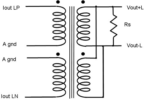
I/V is thanks to a pair of Sowter 1465 I/V transformers with 75r resistors. (there is no issue with the output offset current)
The Sowter I/V transformers are specified for the 1541 and other Dacs used in balanced mode.
You can experiment with secondary load resistors which will alter the primary impedance and this can influence the sound.
There are lots of options that can be experimented with - dem caps, dem oscillator frequency, etc.
I drive my 1541a Dacs with an Iancanada I2S to PCM board in simultaneous mode.
You can experiment with secondary load resistors which will alter the primary impedance and this can influence the sound.
There are lots of options that can be experimented with - dem caps, dem oscillator frequency, etc.
I drive my 1541a Dacs with an Iancanada I2S to PCM board in simultaneous mode.
@batteryman Pls advise a novice: Are bifilar primaries necessary to neutralize the DC offset with dual balanced TDA1541's? Or the balanced connection will cancell the 2mA currents?
The main reason for bifilar windings is to cancel common mode noise and of course offers a x5 or x10 step up so no further amplification or filtering is needed. There is really no point in using a non bifilar wound transformer.
The balanced connection can't cancel the 2ma offset because this is not biploar - flows to ground from each dac so you would need to nullify it with a preset from +5v.
I had a thought as to whether a suitable common mode choke might work as a filter (once the 2ma offset has been nulled)?
The balanced connection can't cancel the 2ma offset because this is not biploar - flows to ground from each dac so you would need to nullify it with a preset from +5v.
I had a thought as to whether a suitable common mode choke might work as a filter (once the 2ma offset has been nulled)?
Ah ok, thanks. And you cancel it with out of phase connected bifilar primaries (wit the center tap to the ground)?The balanced connection can't cancel the 2ma offset because this is not biploar - flows to ground from each dac so you would need to nullify it with a preset from +5v
One DAC will have inverted data so no need to worry about the transformer.
Just connect as below.

Just connect as below.
Ok, so you cancel the DC flux by the primary connection. You mentioned data inversion on one DAC. This is how you achieve your balanced operation? Or you split I2S?
Does anyone know If I use 2 for balanced operation and one chip is R1 and the other is not is that ok?
Here it is 🙂
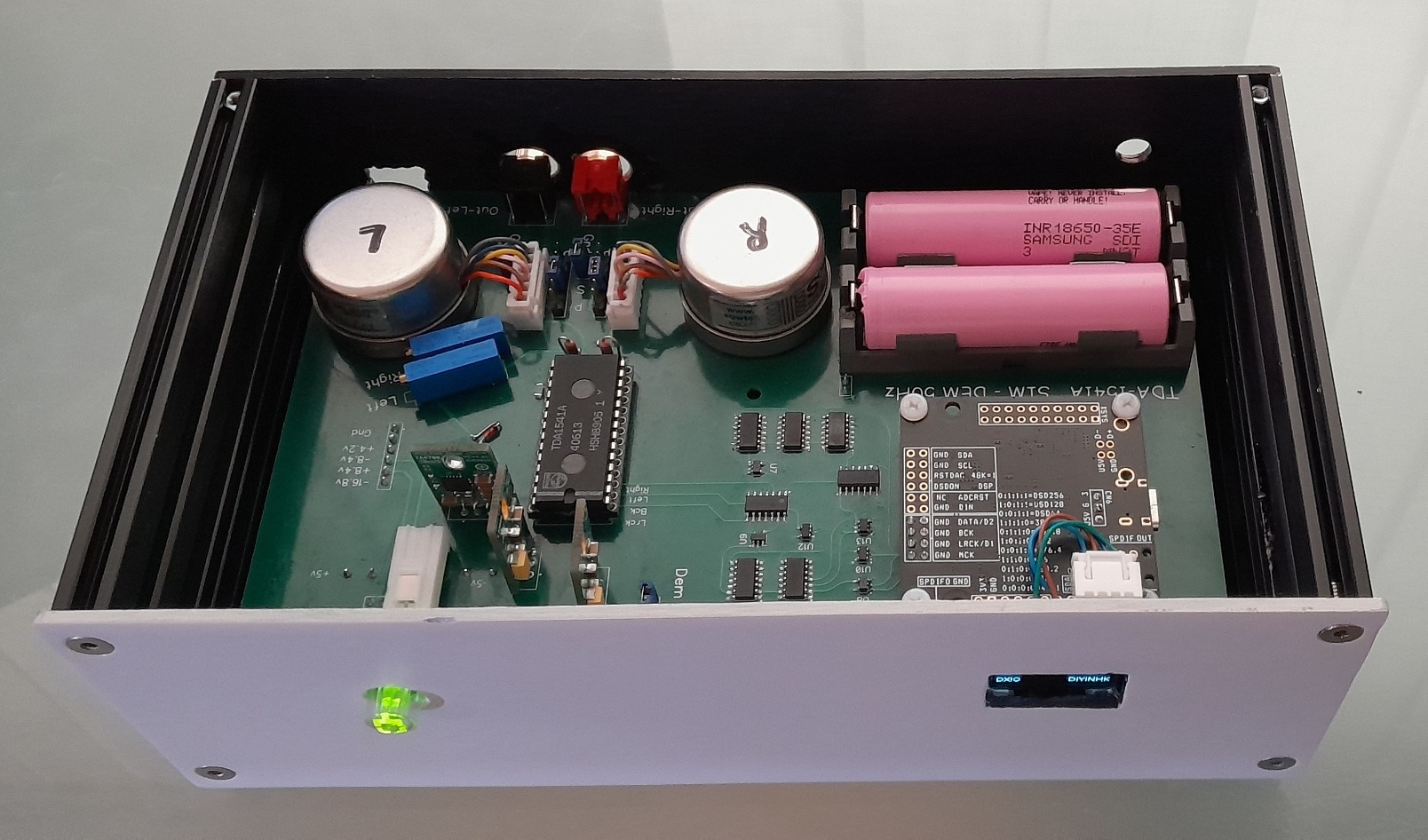
Finally the all thing is in its box , dac batteries are mostly under the pcb , charging post at the rear , one for each voltage , 10 to 15 hours of listening before charging
for the moment I/V resistor are Vishay RN55 47.5 ohm , it's difficult to choose between type of resistor , metal film , carbon , wirewound , etc
a wonderful DAC to listen , highly detailed , superb stereo image , it has tone color ( timbre ) as natural as possible , especially voices , silences are stunning
well , a must have for every audio enthousiaste 😎
.

.
Finally the all thing is in its box , dac batteries are mostly under the pcb , charging post at the rear , one for each voltage , 10 to 15 hours of listening before charging
for the moment I/V resistor are Vishay RN55 47.5 ohm , it's difficult to choose between type of resistor , metal film , carbon , wirewound , etc
a wonderful DAC to listen , highly detailed , superb stereo image , it has tone color ( timbre ) as natural as possible , especially voices , silences are stunning
well , a must have for every audio enthousiaste 😎
.
.
Last edited:
@Zoran is the I2S splitter you tried, the Pedja's circuit with HEF4517 and 74157?It is a bit complicated to make I2S line LL / RR datas. I did it once with some HEF logic. And it was not so bad, (Other DAC chip).
But it was limited speed and deserves 8-12V supply for good operation. Because of "glue logic" used.
...
My tip is that the better way is to use Time Simultaneous format and feed 2 DAC channels inside the TDA1541A with a same data. That will be internal paralleled. DEM oscilator circuit is already the same for booth channels inside the chip.
.
I tried it, and somehow, for me, it was significantly better than I2S classic? (CPLD packed frmat for TDA1540 14bit and optionally 16bit for TDA1541A. Tried both sets.)
I also tried balanced mode with inverted data on other channel of TDA1541A and again, for me, it was not an impovement. It was more noise at measurements, and the sound become somehow "thin" with grainy highs... Balanced digital It is not as analog cancelation...
No it is one designed by myself.
also ECdesign has one with HEFs somewhere in the topic, i think?
If You ask about the power supply prepare to put higher voltages to the HEFs
up to max.
Whatever version You use. It is pretty slow with +5V and cant stand higher Fs
(clicking, kracks, loosong datas etc...)
also ECdesign has one with HEFs somewhere in the topic, i think?
If You ask about the power supply prepare to put higher voltages to the HEFs
up to max.
Whatever version You use. It is pretty slow with +5V and cant stand higher Fs
(clicking, kracks, loosong datas etc...)
Last edited:
What exact EC schematic You use for I2S to Time Simoultaneous format?Finally the all thing is in its box
Thanks ?
Whichever method you use, in my opinion, it must stop bck once the data has been latched.
Analog Devices produced an application note covering this so they must have considered it relevant.
Analog Devices produced an application note covering this so they must have considered it relevant.
- Home
- Source & Line
- Digital Line Level
- Building the ultimate NOS DAC using TDA1541A