Autodetecting timing-chain
Hi all,
Today I did some redesigning of the timing chain. Possible problem was the philips and sony format, since the octal D-I DAC now uses I2S exclusively. So first I designed a I2S format detector, it analyses both BCK and WS, it then outputs a digital signal indicating the format that is applied to the octal D-I DAC, this signal can then be used to automatically adapt both the timing chain and format adapter. Then I tested the new WS timing chain with 3 shiftregisters, it seems to work fine. The 7 BCK WS delay circuit for sony format adaption works fine too. Now all that remains is adding some multiplexers to select the correct taps for the format detected and to enable / disable the 7 BCK WS delay circuit.
So a autodetecting timing-chain can now be constructed that can accept both philips and sony format. The current setup uses 18 HC TTL chip's, I will try to simplify it, but the 18 chip's should already fit on the existing timing-chain module.
I also found some interesting differential I2S buffers. The SY100ELTZG is a dual TTL to PECL differential translator, delay is about 300pS, skew is les than 100pS, that's more like it. The SY100ELT23ZG is the matching dual differential PECL to TTL translator. They both run on 5V and cost around 2 euro's. I2S Input selection could be done using "zero delay" 4:1 demultiplexers type FST3253M.
3 vs 7 logic chips
Lesser chipcount can benefit i guess. Now only 3 for data too? It's a good thing the D-I dac is modular. 🙂
I use 4 shift registers together for delay WS and Data with 4 dacs using. But have some PS troubles to solve first. (LM317/337 pre-reg with TL431 shunts, and shunts are very good for this)
What will the 8 dac D-I dac cost roughly, 2 a 300 Euri's?(not counting the dacs)
(btw: nice diy reed relays! Philips used reed relays for muting on 14 bit players, newer ones had those bad transistors for muting)
I tested a new WS delay circuit yesterday with only 3 shift registers!
Lesser chipcount can benefit i guess. Now only 3 for data too? It's a good thing the D-I dac is modular. 🙂
I use 4 shift registers together for delay WS and Data with 4 dacs using. But have some PS troubles to solve first. (LM317/337 pre-reg with TL431 shunts, and shunts are very good for this)
What will the 8 dac D-I dac cost roughly, 2 a 300 Euri's?(not counting the dacs)
(btw: nice diy reed relays! Philips used reed relays for muting on 14 bit players, newer ones had those bad transistors for muting)
-ecdesigns-,
I was just reading through the entire thread again when it suddenly occurred to me - why did you choose the ECC82/12AU7 type for your tube output stage?
I was just reading through the entire thread again when it suddenly occurred to me - why did you choose the ECC82/12AU7 type for your tube output stage?
Hi adhoc,
Thanks for your reply [post#703]
I used tubes that are available from several suppliers here, I am aware there are better tubes for this purpose but availability could become a problem. I settled for tubes from JJ electronics. I used the ECC82 because of the higher annode current and low impedance needed in the cathode follower, in fact I now use two triodes in parallel, the ECC83 was used for the differential tube amplifier as annode current is much lower here. The tube circuit was optimized using triangle wave shaped test signals.
Today I rewired the octal D-I DAC, using high quality screened wire for both the I/V signals and analog output signals. Aluminum cable ducts and addittional screening was added, only few cables remain visible now. The mains connection between both power supplies also runs trough a aluminum cable duct.
I added a photograph of the octal D-I DAC. I am planning to annodize all interior parts and the tube grille using a gold colour.
Attachments
Hi -ecdesigns-,
So I would be correct to say that your tube output stage now utilises 1x ECC83 and 2x ECC82?
I just found it interesting that you chose the ECC82 as that is not exactly a very 'fashionable' tube. But I think it is a good choice not only due to the reasons you mentioned but another very important one - cost.
Some small signal tube types (think 6SN7 types) are fetching ridiculous prices.
Please do not forget to let me know when PCBs enter production. 😎
New tube amplifier schematics
Hi adhoc,
Thanks for your reply [post#705]
> Yes, you are correct, the tube output stage uses a ECC83 and a ECC82. I promised it anyhow, so I added the new tube amplifier schematics. The 230V preregulated annode voltage enters a shunt stabilizer (R1, D1 and D2), then it is regulated again in a second shunt stabilizer (R2 and D3). This stable reference voltage is used for the annode voltage stabilizers (T1...T4). Due to this setup, hum levels are exeptionally low.
The differential amplifier (V1a and V1b) get's it's bias current from U1, a 2.4mA current source. This current source get's a stable voltage from a cascaded shunt regulator (R14, D4 and R15,D5). I/V output stage voltage is attenuated by R6 / R7 and R11 / R10. Gain is set by R8 and R9, P1 is used to balance the differential amplifier (same DC voltage on both pin 1 and pin 6 of V1).
The cathode follower (V2a and V2b) consists of two triodes in parallell, R5 is a grid stopper. R12 is dimensioned to allow for a high amplitude output signal. C5 is a high quality polypropylene capacitor from Audyn.
The LED's L1 and L2 are status LED's placed directly under the two tubes, mounted in the centre of the tube socket. These LED's are driven with a 0.5 Hz sinewave from a small microcontroller during power-up, and remain lit when the amplifier is operational.
The filament voltage is 12.6V (2 X 6.3V) as pin 9 is not connected, both filaments of each tube are connected in series. The stabilized filament voltage (-12.6V) is generated by the tube power supply, the fCOM is connected to ground, f1 and f2 are connected to -12.6V. During power-up a 18 Ohm resistor limits filament current for all 4 tubes, after gradually heating-up the voltage across the filaments rises due to the increasing filament resistance. Then when the filament voltage exeeds a treshold voltage, a FET shorts the resistor, applying full 12.6V to the filaments, at this moment the annode voltage is switched-on as well. When the tube stage is switched-on while the filaments are still hot, power-up time is much shorter as the treshold is now exeeded much sooner.
As noted before, I use the mixed mode (both op-amp and tube output signals mixed together) exclusively. At the moment I use a 680 ohm resistor between ground and the cinch output, the tube amplifier signal is connected trough a 3.9 KOhm resistor, the op-amp signal trough a 1.8 KOhm resistor. This "mixing" ratio was determined after many hours of listening tests and creates a subtle balance between both signals. Due to the attenuation of both signals, noise levels are reduced to a very low value.
> Sure I will let you know when the Printed Circuit Board's enter production.
Attachments

Hello John!
Bravo to you for doing a very nice job. I am impressed by your mechanical skills as well; the design of the box and machining is very professional...
I have a request though:
Could you please attach a picture of your NOS-DI-DAC's step- or ;even better; Dirac delta- response ?
Thank you in advance.
Keep up the good work.
with regards
Alexiss
Timing chain problems
Hi tubee,
thanks for your reply [post#702]
> No, the DATA delay chain still needs 7 shiftregisters as every single bit has to be delayed. Today another annoying thing occured, the simplified WS timing chain works fine with the philips format, but causes timing problems with the sony format converter, as this one delays WS too. So it looks like there is no easy way around using 7 shift registers for WS as well.
When closely examining the timing chain another problem occured, data sampling on DAC's 2...8. Because data is already sampled by the shift registers on the positive going edge of BCK, it's also synchronized with the positive going edge of BCK, you might run into this problem using a 4 shiftregister delay circuit. So in order for the DAC chip's 2...8 to still work correctly with maximum BCK / DATA skew, BCK for DAC's 2...8 has to be inverted. This way the delayed data for DAC's 2...8 is sampled on the negative going edge of the non-inverted BCK signal.
This introduces a small 177nS delay between DAC1 output and DAC2...8 output.
The philips / sony format detector works fine, the toggling between taps depending on the input format as well.
But due to the problems mentioned above, the automatic detecting timing chain now needs about 22 chip's. Looks like I have to use SMD components.
There is also some good news, I tested the PECL (SY100ELT22 and SY100ELT23) differential drivers / receivers for the I2S interface. Using these in the existing setup, transients are very clean and I couldn't detect any jitter with my oscilloscope anymore, so it must be somewhere below 200pS using a 2.5m interlink and the 4:1 bus switch (FST3253 from Fairchild) included (I use it to switch between four I2S inputs).
The clock buffers for BCK (NC7SZ125) are working fine too, it seems only very high speed / low skew logic prevents adding too much jitter to BCK.
> Octal D-I DAC price, like with the printed circuit boards I want to wait until the design is completed.
Hi Alexiss,
Thanks for your compliments [post#707]
> Yes the housing is comming along fine, it should look even better when it is annodized. Both CNC programming and fixating / aligning parts to be milled takes a lot of time. But not all parts are machined, I had to drill and tap the holes in the side panels manually. Most of the screening parts are also made manually.
> I have already posted many oscillograms of the octal D-I DAC unfiltered output signals, a oscillogram of a squarewave response can be found attached to post#420. I haven't tried recorded triangular or sawtooth shaped signals yet. Basically only the resolution is increased, without affecting phase linearity or increasing the sample rate.
Hello ecdesigns,
In order to find an appropriate low jitter strategy I have some questions ...
a-- are there problems clocking the shift registers at an higer freq. say a typical 11.2896 Mhz ? ( buffered from a CD transport in sync )
b-- what if I set the shift registers clock asinchronous ??
c-- is it possible to achieve good results by generating a BCK signal directly divided/buffered from a good master clock ?
Thanks
Hey what's going on here. Usually, this thread is at the top of the list of the Digital forum. Now it's almost at the bottom.
EC, is the housing finished? Are you still planning to implement USB?
Let's get this party started!
EC, is the housing finished? Are you still planning to implement USB?
Let's get this party started!
Usually, this thread is at the top of the list of the Digital forum. Now it's almost at the bottom.
It is at the top of my list, anyway...
Let the man work at is own (fast) pace.
OT:
Dear Tubelover,
You offered here to sell TDA1541A chips for this project. I know you are busy but you did not answer my mail about a price request.
I think Ecdesigns will not be offended if you post here your price offer. TDA1543 chips will be needed also 😉
This way we will see some action 😀
M.
PWR supply transformers...
Hi again John {ecdesigns} !!
Pray tell, what are the transformers you are using in the power supply? - (I've seen these in a couple of places now...)
ALSO ->>>> Please see Post 554 concerning the 100ohm smd part !
-----> It didn't work !! - NE ideas as 2 why ??
keep up the good work on your new build !!!
L8R,
-Andy-
hi MGH,
I will post the eight pcs of the 1541a chips to u first. U can test with john's untimate deesign.
hi maxlorenz,
I really hadn't received your email. can u email to my another email address thomas_siu@hotmail.com
sorry everyday too many emails. May be some was missing. very sorry for that.
thzx
thomas
Hi MGH,
Thanks for your reply [post#711]
Don't panic 🙂
I have been very busy and didn't have time yet to post new developments, I will try to answer posts as soon as possible.
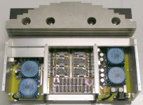
What have I been doing? I just completed the autodetecting dual format timing chain. It has the same dimensions as the old timing chain, yes I managed to get the 3 shiftregister WS timing-chain working. It can detect both Philips and Sony format, then it automatically enables or disables the format converter, configures all tap's and inverts the necessary clock signals. Detecting goes extremely fast, it only needs half a WS cycle. Two LED's indicate the detected format.
The housing is almost finished, the rear panel had to wait for a second problem to be solved. The differential I2S input switch (4 differential I2S channels) and connectors to be used. As you may have read, I tested very fast emitter coupled differential transmitters and receivers. They work very well, meaning almost no added jitter across the I2S interlink, so all I need for the I2S interface is BCK, DATA and WS. The I2S input switch module is almost ready, it uses very fast multiplexers and emitter coupled differential receivers. The chip's used are SMD versions. Channel selection is binary (S0 and S1)
Tomorrow the USB module has to be tested, basically it's the PCM2706 chip with a differential I2S output (emitter coupled logic). I plan to design a very small module that can be directly plugged in the computers USB socket and has a (long) cable that connects to one of the DAC's I2S input's. The most important thing is to obtain exactly the same sound quality with the USB interface as with the reference CD changer.
I added a photograph of the autodetecting timing-chain in action.
Thanks for your reply [post#711]
Don't panic 🙂
I have been very busy and didn't have time yet to post new developments, I will try to answer posts as soon as possible.
What have I been doing? I just completed the autodetecting dual format timing chain. It has the same dimensions as the old timing chain, yes I managed to get the 3 shiftregister WS timing-chain working. It can detect both Philips and Sony format, then it automatically enables or disables the format converter, configures all tap's and inverts the necessary clock signals. Detecting goes extremely fast, it only needs half a WS cycle. Two LED's indicate the detected format.
The housing is almost finished, the rear panel had to wait for a second problem to be solved. The differential I2S input switch (4 differential I2S channels) and connectors to be used. As you may have read, I tested very fast emitter coupled differential transmitters and receivers. They work very well, meaning almost no added jitter across the I2S interlink, so all I need for the I2S interface is BCK, DATA and WS. The I2S input switch module is almost ready, it uses very fast multiplexers and emitter coupled differential receivers. The chip's used are SMD versions. Channel selection is binary (S0 and S1)
Tomorrow the USB module has to be tested, basically it's the PCM2706 chip with a differential I2S output (emitter coupled logic). I plan to design a very small module that can be directly plugged in the computers USB socket and has a (long) cable that connects to one of the DAC's I2S input's. The most important thing is to obtain exactly the same sound quality with the USB interface as with the reference CD changer.
I added a photograph of the autodetecting timing-chain in action.
Attachments
-ecdesigns- said:
I plan to design a very small module that can be directly plugged in the computers USB socket and has a (long) cable that connects to one of the DAC's I2S input's.
I hope you are not going to have the USB Interface powered by the PC, are you ?? 😱
doede
Hi NjoyTHEMUSIC,
thanks for your reply [post#713],
The transformers are encapsulated torroid transformers with both very low hum and low external magnetic field. I also used them in the twin DAC. They are from Nuvotem Talema, and can be ordered at Digikey or RS components.
Yes, the resistor was placed correctly, if the motor starts spinning fast, the clock signal amplitude is too low, or the clock signal is missing. Looks like the Trichord module can't provide enough current (it's output impedance is too high, or something is wrong with the ground return path). In that case there is no choise but removing the terminating resistor like you already did. With a good clock buffer it shouldn't be a problem to drive loads as low as 50 Ohms.
cheers,
John
Thanks Thomas, I'll be waiting for the chips. When will you ship?
Thanks EC, good to hear you've made more progress. As Doede implies, powering the USB module by the PC may not be a good idea. Have you considered using the CM106L instead of PCM2706? Little more expensive but suppose to be a better.
Thanks EC, good to hear you've made more progress. As Doede implies, powering the USB module by the PC may not be a good idea. Have you considered using the CM106L instead of PCM2706? Little more expensive but suppose to be a better.
USB interface
Hi dddac,
Thanks for your your reply [post#716]
No I am going to try self powered mode first (with a 3.3V regulator) on various computers, if this works correctly, I am going to do some tests if I can filter the USB voltage enough to obtain a clean power supply for the SpAct PLL circuitry. Another option is synchronously reclocking, then jitter is determined by the stability of the clock source of the USB chipset. If the mac / PC USB power supply cannot be filtered enough, I can use a very small dedicated power supply (adapter) with a ringcore transformer.
I choose this setup because the USB interlink has to be as short as possible to avoid addittional jitter. I tested the differential PECL I2S interface with a 10m interlink, and it works fine. I tested both 50 and 120 Ohm termination.
Hi stefanobilliani,
Thanks for your reply [post#710]
> I presume you are referring to the timing chain? The shift-registers used should be fast enough to run on 11.2896 MHz, but as I previously noted, ALL DAC's that receive delayed WS and DATA must receive a inverted clock, NBCK. Only the first DAC chip that connects directly to both WS and DATA receives BCK.
> If the shift registers (timing chain) are clocked asynchronous, data corruption might occur. If the I2S reclocking circuit is clocked asynchronous, continuously varying jitter is minimized, but BCK now "jumps" between the nearest master clock transients, still the perceived sound quality is usually better than with continuously varying jitter.
> When BCK has the same frequency as the master clock this should be possible. If I am correct, dividing BCK can cause loss of synchronization.
- Home
- Source & Line
- Digital Line Level
- Building the ultimate NOS DAC using TDA1541A