Main power supply silkscreen plot
Hi all,
I added a main power supply silkscreen plot.
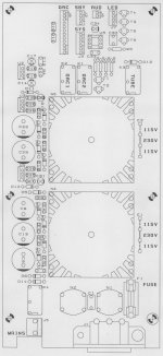
Mains socket is at the bottom right of the circuit board. A fuse protects both power supplies. Both transformers are sealed torroid types (Nuvotem-Talema) of 25VA (N3) and 15VA (N5). Mains voltage selection is on the right of both transformers, for 230Vac the 230V jumper has to be soldered, for 115Vac, both 115V jumpers have to be soldered, the 230V jumper is removed. J5 routes the switched mains voltage to the tube power supply, a gap is provided in the circuit board to allow this cable to be routed trough a aluminum cable duct. Connections are on top, DAC are the DAC output voltages: -8V, +8V, -20V and +20V. SBY is the +8V stand-by and auxilary voltage, SYS is connected to the system controller, AUD is the tube operational switch signal and LED is the connector for the status LED's. This power supply is placed at the left-hand side of the octal D-I DAC when viewed from the front. U2,3,4 need some minor cooling, it's provided by a small heatsink. When the differential tube output is not used, components necessary for this part can be left out (C32..34, D14, J5...J7, K4, R3...5, T2...T6, U5).
Hi all,
I added a main power supply silkscreen plot.
Mains socket is at the bottom right of the circuit board. A fuse protects both power supplies. Both transformers are sealed torroid types (Nuvotem-Talema) of 25VA (N3) and 15VA (N5). Mains voltage selection is on the right of both transformers, for 230Vac the 230V jumper has to be soldered, for 115Vac, both 115V jumpers have to be soldered, the 230V jumper is removed. J5 routes the switched mains voltage to the tube power supply, a gap is provided in the circuit board to allow this cable to be routed trough a aluminum cable duct. Connections are on top, DAC are the DAC output voltages: -8V, +8V, -20V and +20V. SBY is the +8V stand-by and auxilary voltage, SYS is connected to the system controller, AUD is the tube operational switch signal and LED is the connector for the status LED's. This power supply is placed at the left-hand side of the octal D-I DAC when viewed from the front. U2,3,4 need some minor cooling, it's provided by a small heatsink. When the differential tube output is not used, components necessary for this part can be left out (C32..34, D14, J5...J7, K4, R3...5, T2...T6, U5).
Attachments
Tube power supply schematics
Hi all,
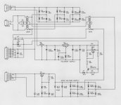
Next is the tube power supply schematics.
When the main power supply applies the mains voltage to the tube power supply, transformer N1 get's power. The ac voltage is rectified and split up in 2 voltages, +20V and -20V, but the +20V is connected to ground. So on the annodes of D2 and D4 we get about -40V, this voltage is used for the current source in the differential tube stage. The transformers centre tap now carries -20V with respect to ground, this voltage is applied to a negative voltage regulator for the filament voltage (U1), with the diode connected to common, approx. -12.6V filament voltage with respect to ground is obtained.
The filaments of the ECC82 / ECC83 use the internal series connection, so they run on 2 X 6.3V = 12.6V. However, R1 drastically limits the filament current, so the voltage across the filaments starts rising slowly. This is caused by the fact that a cold filament has a much lower resistance than a heated filament. When the filament slowly heat's up, the voltage at some time exeeds the reference voltage set by the zenerdiode D7. Now T2 starts conducting and pulls the gate of N-channel mosfet T1 to the plus (ground), T1 short circuits R1 (low RDSon) and the pre-heated filaments now receive the full 12.6V. But now the voltage is also high enough to trigger relay K1 (12V relay), K1 in turn connects the secundary winding of N1 (2 X 18Vac) to the secundary winding of N2, with this setup N2 now boosts the 2 X 18Vac to approx. 220Vac. This voltage is rectified and then pre-stabilized by the high-voltage mosfet T3 to approx. 220V.
This way a smooth sequential power-up of both the filament supply and the HV supply is ensured, and only two standard encapsulated torroid transformers are needed to run both tube output modules.
The output voltages for both filaments and HV are very smooth, avoiding hum.
Hi all,
Next is the tube power supply schematics.
When the main power supply applies the mains voltage to the tube power supply, transformer N1 get's power. The ac voltage is rectified and split up in 2 voltages, +20V and -20V, but the +20V is connected to ground. So on the annodes of D2 and D4 we get about -40V, this voltage is used for the current source in the differential tube stage. The transformers centre tap now carries -20V with respect to ground, this voltage is applied to a negative voltage regulator for the filament voltage (U1), with the diode connected to common, approx. -12.6V filament voltage with respect to ground is obtained.
The filaments of the ECC82 / ECC83 use the internal series connection, so they run on 2 X 6.3V = 12.6V. However, R1 drastically limits the filament current, so the voltage across the filaments starts rising slowly. This is caused by the fact that a cold filament has a much lower resistance than a heated filament. When the filament slowly heat's up, the voltage at some time exeeds the reference voltage set by the zenerdiode D7. Now T2 starts conducting and pulls the gate of N-channel mosfet T1 to the plus (ground), T1 short circuits R1 (low RDSon) and the pre-heated filaments now receive the full 12.6V. But now the voltage is also high enough to trigger relay K1 (12V relay), K1 in turn connects the secundary winding of N1 (2 X 18Vac) to the secundary winding of N2, with this setup N2 now boosts the 2 X 18Vac to approx. 220Vac. This voltage is rectified and then pre-stabilized by the high-voltage mosfet T3 to approx. 220V.
This way a smooth sequential power-up of both the filament supply and the HV supply is ensured, and only two standard encapsulated torroid transformers are needed to run both tube output modules.
The output voltages for both filaments and HV are very smooth, avoiding hum.
Attachments
Tube power supply silkscreen plot
Hi all,
I added the tube power supply silkscreen plot.
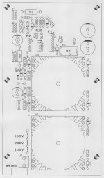
Mains voltage enters J2 at the bottom left of the circuit board. Both transformers are sealed torroid types (Nuvotem-Talema) of 25VA (N1) and 15VA (N2). Mains voltage selection is on the left of N1, for 230Vac the 230V jumper has to be soldered, for 115Vac, both 115V jumpers have to be soldered, the 230V jumper is removed. Connections are on top, HV is the +220V supply, -V is the -40V supply for the current source and FIL carries the -12.6V filament voltage. This power supply is placed at the right-hand side of the octal D-I DAC when viewed from the front. U1 needs sufficient cooling and is mounted to the right-hand side aluminum side panel, together with T1 and T3. Just like the main power supply, the tube power supply is mounted on 2 massive aluminum bars using 3 screws on each side. Transformers are firmly fixed to the printed circuit board using M4 screws at the centre.
Hi all,
I added the tube power supply silkscreen plot.
Mains voltage enters J2 at the bottom left of the circuit board. Both transformers are sealed torroid types (Nuvotem-Talema) of 25VA (N1) and 15VA (N2). Mains voltage selection is on the left of N1, for 230Vac the 230V jumper has to be soldered, for 115Vac, both 115V jumpers have to be soldered, the 230V jumper is removed. Connections are on top, HV is the +220V supply, -V is the -40V supply for the current source and FIL carries the -12.6V filament voltage. This power supply is placed at the right-hand side of the octal D-I DAC when viewed from the front. U1 needs sufficient cooling and is mounted to the right-hand side aluminum side panel, together with T1 and T3. Just like the main power supply, the tube power supply is mounted on 2 massive aluminum bars using 3 screws on each side. Transformers are firmly fixed to the printed circuit board using M4 screws at the centre.
Attachments
Timing
Hi John.
Nice HT , simply with a BUZ.
Last days i printed all layouts and studied them. Even on a laser printout some things are difficult to read. But i have a good impression.
2 questions:
>Dac 1 gets a direct I2S signal, but the other 7 dacs get it through 166 logic chips. With this on my mind:
>Can the differential hybrid output stage be used with a standard single ended cinch pre-amp input? (Use only one halve of it?)
I have allmost finished my 4 shift register logic to test my 4 1541's setup. Yes i am stubborn, want to hear it how its sounds. All dacs get data & WS from 74/164's
But first i will have a holiday.
Hi John.
Nice HT , simply with a BUZ.
Last days i printed all layouts and studied them. Even on a laser printout some things are difficult to read. But i have a good impression.
2 questions:
>Dac 1 gets a direct I2S signal, but the other 7 dacs get it through 166 logic chips. With this on my mind:
In the D-I setup 1 dac is direct feeded, and 7 dacs get their I2S slightly delayed. Imo all dacs should get their I2S by the same logic to reduce timing errors.When reclocking, all I2S signals must be reclocked to keep delay times equa
>Can the differential hybrid output stage be used with a standard single ended cinch pre-amp input? (Use only one halve of it?)
I have allmost finished my 4 shift register logic to test my 4 1541's setup. Yes i am stubborn, want to hear it how its sounds. All dacs get data & WS from 74/164's
But first i will have a holiday.
To reduce diode noise in PS, 1N4007 could be modified to BYV95C, or other soft recovery types. I have done that a three times now (PS from tube headphone amp - preamp - ps in CDP) First i did not believe in this upgrade, but this is really worth a try. Hybrid poweramp will be modified too in time (PS of tube section, and eight HFA08TB60's in low voltage section)
The whole is sounding "faster" with BYV's compared to 1N4007's and give a better depth in soundstage.
(I removed the caps bypassing the diodes too)
see also:
http://home.hccnet.nl/r.r.meijer/pdf/diode 1.pdf
http://home.hccnet.nl/r.r.meijer/pdf/diode 2.pdf
(copied from a CD882 modifier)
The whole is sounding "faster" with BYV's compared to 1N4007's and give a better depth in soundstage.
(I removed the caps bypassing the diodes too)
see also:
http://home.hccnet.nl/r.r.meijer/pdf/diode 1.pdf
http://home.hccnet.nl/r.r.meijer/pdf/diode 2.pdf
(copied from a CD882 modifier)
If this design ever comes to DIY fruition, count me (along with MGH eh? 😉) as people more than willing to be one of the first brave few to try this out.
I am more than willing to pay a little extra for a superlatively constructed PCB. I'm thinking extra thick copper traces, with gold plating on Teflon here.
I am more than willing to pay a little extra for a superlatively constructed PCB. I'm thinking extra thick copper traces, with gold plating on Teflon here.
Bernhard,Bernhard said:Until today I have tested four S1 from CD players, six S1 NOS and one S2 NOS.
Only one S1 from CD player was good, the rest was good on one channel only or not good at all.
Could you please elaborate on the problems you encountered with the various NOS TDA1541As?
I find it extremely worrying as I am about to pick some of these chips soon. Does the TDA1541 have a high failure rate? What constitutes 'not good' for you?
Cheers.
-Aaron
Hi John, 🙂
I saw you intend to use 78/79XX type of regulators. In my limited experience, LM317/337 or 1086 regulators, with a good cap bypassing ADJ pin, give a significant enhancement in sound quality and add only a little price increase.
Aaron wrote:
Maybe for power PCB's but for the digital circuits maybe it will be bad?
Are there OCC copper or silver PCB's?? 😀 (Ohno Continuous Cast Copper; wire sounds extremelly good.)
Keep the excellent work, John.
M
I (we) didn't want to put pressure on you, just showing our interest in your work.Yes, the printed circuit boards. I am still testing and optimizing the octal D/I DAC, this could result in redesingning one or more circuit boards for optimal results / optimal flexibility. Each design needs to be checked very carefully to avoid errors during manufacturing.
I saw you intend to use 78/79XX type of regulators. In my limited experience, LM317/337 or 1086 regulators, with a good cap bypassing ADJ pin, give a significant enhancement in sound quality and add only a little price increase.
Aaron wrote:
I'm thinking extra thick copper traces,
Maybe for power PCB's but for the digital circuits maybe it will be bad?
Are there OCC copper or silver PCB's?? 😀 (Ohno Continuous Cast Copper; wire sounds extremelly good.)
Keep the excellent work, John.
M
adhoc said:
Bernhard,
Could you please elaborate on the problems you encountered with the various NOS TDA1541As?
I find it extremely worrying as I am about to pick some of these chips soon. Does the TDA1541 have a high failure rate? What constitutes 'not good' for you?
Cheers.
-Aaron
Aaron,
"not good" means that the results of the measurments of the crown chips have not been much better or not better at all than those of plain 1541As.
I can not remember any dead TDA1541A.
John,
an "ultimate DAC" deserves a better power supply for the Tube stage. I have build this version many times and it for sure will benefit from soft recovery diodes and a RC section in stead of only the C section after the BUZ80.
Real good results you will only get (in comparison with the solid state version) with a tube rectifier and a C-L-C filter with high quality components....
Differences occur mostly in les sharp highs and a more open transparent soundstage. All those things you try to achieve with a very complex and costly DAC design, so lets not "save" on the tube stage than is my motto
Same applies for the opamp power supply imho
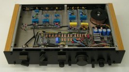
Power supplies assembled
Hi all,
Project update,
I have manufactured both power supply printed circuit boards today. Then I assembled them both, machined some more chassis parts and put it all together to see if everything would fit. I added a photograph to give a impression of how it looks like.
Hi all,
Project update,
I have manufactured both power supply printed circuit boards today. Then I assembled them both, machined some more chassis parts and put it all together to see if everything would fit. I added a photograph to give a impression of how it looks like.
Attachments
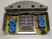
I have manufactured both power supply printed circuit boards today. Then I assembled them both, machined some more chassis parts and put it all together to see if everything would fit.
WOW!


Because of pictures like yours I don't need to visit triple-X sites any more 😀
M
building ultimate dac
John, This dac is awesome & breathtaking!! I want to be on your list to purchase one when you commence to offer these to the DIY gang. It is refreshing to see the pure energy of one's love put into a product in todays world of "mediocrity"! Again, thx for a superb job WELL DONE!! Regards Ronnie
John, This dac is awesome & breathtaking!! I want to be on your list to purchase one when you commence to offer these to the DIY gang. It is refreshing to see the pure energy of one's love put into a product in todays world of "mediocrity"! Again, thx for a superb job WELL DONE!! Regards Ronnie
Hi tubee,
Thanks for your reply [post#684]
> The most important signal for low jitter is BCK as it determines when the next sample appears at the DAC output. All DAC chip's 1...8 get BCK trough the same logic, at the same time. Both WS and DATA are delayed for the other 7 DAC chip's, timing of both WS and DATA only has to be accurate enough to prevent data corruption.
When reducing jitter, BCK can be synchronously reclocked (at the transport) using MCK that runs synchronously with I2S. Only BCK needs to be reclocked to reduce jitter, but by doing so, it is delayed 2 MCK cycles with respect to both WS and DATA. Now WS and DATA are not correctly aligned wit BCK any longer. To overcome this problem, both WS and DATA are reclocked in a similar way as BCK, so they will also get 2 cycles delay. Now all I2S signals are correctly aligned again.
> The differential hybrid output stage (both op-amp and tube) have single ended outputs and can be connected to a cinch preamp input, I am using the same setup as well. The DAC chip's are arranged differential, one DAC group (1,3,5,7) carry the non-inverted signal, the other DAC group (2,4,6,8) carry the inverted signal (serial DATA is inverted). So a differential stage is needed to add the signals from both group's together again. This is done to achieve a DC coupled signal and reduce interference.
[post#686]
Yes, I will try some different diodes. I have some BYV27-400 (ultra fast controlled avalanche rectifiers, 25nS) and BYV95C.
Octal D-I DAC migration
Hi tube-lover,
Thanks for your compliments [post#685]
Today the octal D-I DAC migrated from the breadboard setup to the new aluminum housing. After some troubles with the main power supply module, everything is working perfectly now. I will post some more pictures later.
Hi tube-lover,
Thanks for your compliments [post#685]
Today the octal D-I DAC migrated from the breadboard setup to the new aluminum housing. After some troubles with the main power supply module, everything is working perfectly now. I will post some more pictures later.
Hi adhoc,
Thanks for your reply [post#687]
Thicker copper traces are no problem, gold plating seems to become standard due to the RoHS directive (other platings gave too much problems).
However, I used standard printed circuit boards in my 20 years-old control amplifier, and they still work perfectly.
I added a photograph of this "oldtimer", one printed circuit board was removed to install a different op-amp. All printed circuit boards are double sided and sprayed with a grey primer. Only one channel is visible, the other channel is mounted at the other side for optimal channel separation. The coils are reed relays, I made them myself. I used coil formers from philips coils and put a new winding on them, I removed the ferrite core and inserted a reed contact. As you can see, I was already using modular setup's 20 years ago. The wooden side panels are of massive oak of course. I also made all chassis parts and knobs myself.
Attachments
Hi maxlorenz,
Thanks for your compliments [post#689]
> Well, one module could be redesigned now to enhance functionality. I tested a new WS delay circuit yesterday with only 3 shift registers! Now there is more space on the timing chain module, so maybe I could integrate a format converter. This way a universal timing-chain could be constructed that can handle both the philips and the sony format.
> The 78/79XX regulators are used as pre-regulators, the tube output modules have integrated cascaded zener stabilizers. The first zenerdiode stabilizes the voltage, but a small ripple remains, now this voltage is used to bias a second zenerdiode to keep ripple extremely low. A discrete stabilizer circuit is used for each annode. The op-amp circuit also has a pre-regulator on the main power supply and a local regulator on the module. I will experiment with other types for the local regulator, as soon as the main setup is ready.
WS timing chain with 3 shiftregisters
Hi dddac,
Thanks for your tip [post#691]
> I will post the new tube output stage schematics soon so you can have a look how both tube power supply pre-regulator and local regulators are set up.
If soft recovery diodes can reduce switching noise, I will use them of course.
> I use the octal D-I DAC with mixed mode exclusively now, only tube or only op-amp doesn't sound as good once you heard the mixed mode.
> The op-amp power supply is a pre-regulator as well, the actual regulator is integrated in the op-amp module. That one could be optimized of course.
I also didn't forget your tip about simplifying the WS delay circuit [post#52], I know it sometimes seems as if I don't take every tip into account, but actually I do. It has resulted in a WS delay chain using only 3 shift registers instead of 7. The problem was to perfectly synchronize the divide by 8 counter with both WS and BCK, so I used two shiftregisters with feedback for this purpose instead. The third shiftregister is now clocked with the divide by 8 signal that always runs synchronous with both BCK and WS. It then outputs the 7 delayed WS signals: WS8, WS16, WS24, WS32, WS40, WS48 and WS56. Even more interesting is the capability to switch between format's, by changing the feedback loops, both philips format (8BCK delay) or sony format (6BCK) delay can easily be selected for WS, without changing the taps. I will post some schematics soon
Hi EC
that looks really very nice, still I wonder if linearity is affected by new samples....
Today I made a comparison between a Philips CD960 with a known good TDA1541A S1 in non os and a Sony CDP 502ESmkII with a pair of BurrBrown instrumentation DACs that are pin compatible to PCM53, also in non os.
My impression of the Philips was much the same like when I tried that over a year ago:
On one hand it sounds full and sweet (warm), compared to 4x os with SAA7220B, but on the other hand muddy and blown up.
The spectrum analyzer shows what happens here:
with low level test signal, the harmonics in 4x os are all <= -60dB, but in non os the even harmonics K2, K4, K6, K8 rise about 10dB to -50dB. They stand clearly visible above the noise floor which is -60dB without averaging.
What you see is what you hear or vice versa 😀
The Sony sounds much more neutral, while preserving the positive effects of non os.
I found that the linearity of BB chips is not as much affected by non os, a good PCM56 has -65dB in 8x os and -60dB in non os, which is acceptable because -60dB harmonics are hidden in a -60dB noise floor.
Non os might be an improvement for the plain TDA1541A because with the SAA7220B there is a strong K5 which sounds harsh and unpure.
What has it got to do with your DAC ?
When you have time, try PCM56 with MSB adjust.
- Home
- Source & Line
- Digital Line Level
- Building the ultimate NOS DAC using TDA1541A