power supply modules
Hi all,
Project update,
Currently the octal D-I DAC power supplies are being developed. There will be 2 separate power supply modules, the main power supply for the DAC and the separate tube power supply. The main power supply also provides the stand-by supply by using a addittional rectifier. The main power supply generates the following (pre-regulated) voltages:
-10V, +10V, -25V, +25V and +10V stand-by voltage
It also includes a small microcontroller (PIC12F629) in a DIP8 package (similar to the TDA1543) with a on-chip oscillator (no crystal needed). It will drive the 4 LED tube status indicator's (2 Hz sinewave pattern during warming-up). It also controlls the tube power supply start-up and shut-down sequence for both filament and HV using PWM output's and relay output's. A input pin is provided for shutting-down the tube stage (op-amp mode only).
Relay's are used to shut down the main supply in stand-by mode.
The tube power supply provides the stabilized filament DC voltage, the -50V for the current sources and the stabilized 250V HV. Both HV and filament supplies have separate relay's for sequential power-up / power-down. In addittion PWM signal from the microcontroller ensure correct soft-start operation for both, the filament and HV supply.
Both power supply modules are mounted on massive 1 x 1 cm aluminum bar's that support the circuit board's on both sides for optimal mechanical strength. Neoprene rubber strips are placed between circuit board and the aluminum bar's for suppressing mechanical noise (transformer hum and relay switching sound's)
Re: PCM56
The PCM56 works very good without deglitcher.
I tried 1541A non os in CD880, CD960 and CD650, just removed the os, nothing else.
OT:
Why not mis-use a deglitcher for reclocking ?
That would eliminate all jitter including that from logic inside DAC.
-ecdesigns- said:Hi Bernhard,
Thanks for your reply [post#653]
The PCM56 cost about 13...16 euro's each, so when it's performance prooves to be equal or better than the double crown TDA1541A during listening sessions, it's a good alternative. The PCM56 uses a resistive ladder network for D/A conversion. Problems occur especcialy at the 011...11 to 100..00 changeover, the datasheet also includes a deglitcher circuit, so problems of this nature are already expected.
The TDA1541A however uses a technique to avoid these errors. The linearity errors are a different aspect. You mentioned the TDA1541A used in a NOS setup produces a sound that's too warm. What type of output circuit was used?
The PCM56 works very good without deglitcher.
I tried 1541A non os in CD880, CD960 and CD650, just removed the os, nothing else.
OT:
Why not mis-use a deglitcher for reclocking ?
That would eliminate all jitter including that from logic inside DAC.
Thanks EC,
Now I get it ... not having to use a coupling cap if you use a single ended output in DC coupled design.
Will the PCB going to have doubled sided trace?
Do you know the output impedence of the Octal D-I DAC? I have a integrated tube amp with a passive stepped attenuator (50 kOhm input impedence).
Now I get it ... not having to use a coupling cap if you use a single ended output in DC coupled design.
Will the PCB going to have doubled sided trace?
Do you know the output impedence of the Octal D-I DAC? I have a integrated tube amp with a passive stepped attenuator (50 kOhm input impedence).
Great work, ecdesigns,
Can I take the output from the balanced stage opamps directly to my transformer based volume control, DC coupled?
Will the + and - signal from each channel match exactly?
Thanks
M
> The balanced DAC design is mainly used to create a fully DC coupled output without capacitors or transformers as they can affect sound quality. A wire still has the lowest distortion. When the DC coupled output is created, it is applied to a single ended RCA connector.
Can I take the output from the balanced stage opamps directly to my transformer based volume control, DC coupled?
Will the + and - signal from each channel match exactly?
Thanks
M
I2S connector?
John i have been thinking of a I2S connector from CD engine to dac. Maybe a simple 9 or 15 pins D-connector could do the job. With this solution you have a rather good, sheap connection, shielding possible too. And pins left to lead a master clock signal back top CD engine. A small mini-Din would do too, but has not enough pins.
John i have been thinking of a I2S connector from CD engine to dac. Maybe a simple 9 or 15 pins D-connector could do the job. With this solution you have a rather good, sheap connection, shielding possible too. And pins left to lead a master clock signal back top CD engine. A small mini-Din would do too, but has not enough pins.
hi all,
for update only, if any diyers like to build john's ultimate design 1541a pls email for me about the same date code chips.
Today I check my stock of 1541a chips. still had some 88~91 date code can match 8~16 pcs same date code & same s/n.
BTW, assistance by peter. I can get the good price of 1541a double crown 1541AS2.
now will USD 80 per chip. include all charge, I will use regmail post to all diyers. Over 2 chips I will suggest use insurance parcel. This price was almost same as three years before.
thx
thomas
Hi MGH,
Thanks for your reply [post#663]
> Yes the printed circuit boards will have track's on both sides. I am not sure if only the pad's are gold plated or the track's as well. If the track's have to be gold plated anyway, a transparent anti solder mask would look nice.
> The output impedance of the octal D-I DAC using mixed mode is about 600 Ohms, however if necessary, it can be lowered. The main "problem" is the tube output stage, if I put a addittional buffer (opa627) after the mixed mode output (same happens already in my control amplifier), the output impedance can be much lower. In this case, the mixing ratio between tube and op-amp output signal has to be changed. I now use a very short interlink (40cm) between DAC and control amplifier, The average input impedance of my control amplifier is 40 KOhm. So the 50 KOhm input impedance of your stepped regulator should not be a problem.
output impedance
Hi maxlorenz,
thanks for your reply [post#664]
The octal D-I DAC, using mixed mode has about 600 Ohm output impedance, single ended. Another option is to add a buffer op-amp at the octal D-I DAC output to achieve very low output impedance, as I explained in post #667. The maximum offset voltage on the single ended output is about 10mV.
I am just curious about a transformer based volume control, what is the advantage over a pure resistive stepped attenuatur using high quality low noise resistors?
Modular high-speed I2S buffer
Hi tubee,
Thanks for your reply [post#665]
> The connectors that I had in mind are 8 way DIN connectors with screen, so 4 differential signals can be used (clock included). They are not that expensive and smaller than a sub-D connector. To mount them in a chassis, only one 18mm hole has to be drilled. The metal housing of the plug has a mat chrome finish and a screw lock. The socket is made of massive aluminum. I used these connectors over the last 16 years in various projects and they proove to be very reliable.
I found a very interesting buffer for I2S signals, it's the NC7SZ125 from Fairchild. It has a very small 5 pin SMD housing with one single buffer, typical delay is 2.6nS, it can run on 5V as well. I already designed a adapter circuit board containing 3 of these buffers (14 pin DIP size). So it can be used in the existing timing chain, or as a modular high speed I2S buffer.
The mini clock upgrade circuit board has been modified too, it now has the NC7SZ125 integrated.
Both the program for the PIC12F629 and the printed circuit board design for the main power supply are ready. The tube status LED's are driven with a 0.5 Hz sinewave, produced by the microcontroller (PWM), this looks very impressive. The LED's pulsate slowly until the tube output stage is operational, then they switch-on and the tube output signal is added to the op-amp signal.
Yet another technique is used for limiting the filament inrush current, as the constant current sources used too much power. After switching-on the filament current is limited by a resistor, as the filaments start heating-up, the voltage across them increases. Now at a specific treshold, the resistor is bypassed by a mosfet switch, and the full 12.6V is applied to the filaments. At this moment the filament voltage suddenly increases, driving a 12V relay that switches-on HV as well. Due to power supply modifications, power consumption of the complete octal D-I DAC, including tube output stages is down to about 40W. Stand-by power is very low <1W.
As the TDA1541A's get quite hot with the current high temperatures over here at my place (32 degrees centigrade). I looked for IC heatsink's and found them at Farnell, they come in two versions, for 24 pin and 40 pin IC's. Both types can be used with the analog mainboard setup.
I also found a very interesting article about the Non-oversampling Digital filter-less DAC Concept (Ryohei Kusunoki) on the internet.
It notes jitter values for NOS DAC's should not exeed 173pS, and for a 8 times oversampling DAC jitter should not exeed 1.35pS!
Hi ecdesigns,
Thanks for your reply 🙂 (post #668)
I did not explain myself well (or I totally misundertsood you).
On post nº50 you showed a diagram for the output section of a opamp-only D-I DAC (probably my choice). On it, I/V is based on paralleled (inverting) OPA627 for each channel, then a differential opamp is added to end with single ended, DC coupled output. Am I wright?
My question was about saving this last differential opamp and taking the output straight from the I/V stage, DC coupled, to a XLR connector. Then my TVC should make the "differential" part of it, provided -DC and +DC are of equal magnitude. Am I totally wrong here???🙁
Appart the fact that OPA627AP are expensive (US$8.25 here at the market place 😉 ) , I like the simpler way...
From a non-technical music lover:
1) Galvanic isolation.
2) When attenuating, TX's makes V for I conversion with little heat generation while R loose energy as heat. It is said (and I agree ) that this allow for more "balanced" sound presentation even at lower volumes (higher current) maintaining bass output and dynamics. With a high Vout DAC, a TVC excells 😎
3) Allows for easy conversion from single ended to balanced and vice versa.
4) Sound?
That said, I am also very pleased with "Kookaburra" from the guys at twistedpairaudio.com wich has Burr-Brown PGA2311PA Stereo Analog Volume Control.
For more info, please goto:
http://www.stevens-billington.co.uk/pagehifi.htm
http://www.mfaudio.co.uk/
Unfortunatelly, they are expensive
Sorry guys for distracting the man
Best wishes,
M
Thanks for your reply 🙂 (post #668)
The octal D-I DAC, using mixed mode has about 600 Ohm output impedance
I did not explain myself well (or I totally misundertsood you).
On post nº50 you showed a diagram for the output section of a opamp-only D-I DAC (probably my choice). On it, I/V is based on paralleled (inverting) OPA627 for each channel, then a differential opamp is added to end with single ended, DC coupled output. Am I wright?
My question was about saving this last differential opamp and taking the output straight from the I/V stage, DC coupled, to a XLR connector. Then my TVC should make the "differential" part of it, provided -DC and +DC are of equal magnitude. Am I totally wrong here???🙁
Appart the fact that OPA627AP are expensive (US$8.25 here at the market place 😉 ) , I like the simpler way...
I am just curious about a transformer based volume control, what is the advantage over a pure resistive stepped attenuatur using high quality low noise resistors?
From a non-technical music lover:
1) Galvanic isolation.
2) When attenuating, TX's makes V for I conversion with little heat generation while R loose energy as heat. It is said (and I agree ) that this allow for more "balanced" sound presentation even at lower volumes (higher current) maintaining bass output and dynamics. With a high Vout DAC, a TVC excells 😎
3) Allows for easy conversion from single ended to balanced and vice versa.
4) Sound?
That said, I am also very pleased with "Kookaburra" from the guys at twistedpairaudio.com wich has Burr-Brown PGA2311PA Stereo Analog Volume Control.
For more info, please goto:
http://www.stevens-billington.co.uk/pagehifi.htm
http://www.mfaudio.co.uk/
Unfortunatelly, they are expensive
Sorry guys for distracting the man
Best wishes,
M
John, nice features on the new designed PS. I like the filament-solutions, combined with switching of HT.
Is it allways worthwile to reclock I2S, or is clock signal only enough? But if jitter may not exceed 1.35pS, reclocking is a must then? I cannot measure jitter here, have a loan 20Mhz scope only, and its diificult to get a lock on 11 mhz.
Comparing jitter with (a modified) master clock is still comparing the signal with a possible jittering reference. Better way would be a allmost jitter-free reference clock to compare all other signals with.
Thanks EC.
A gold plated PCB with transparent mask would look really nice. I would get a clear cover for the housing so you can see the beautiful work inside.
600 ohm is the standard for balanced XLR output, I think. In my experience, the lower the output impedence more dynamic the sound especially with passive preamps.
Hi maxlorenz,
Thanks for your explanation [post#670]
> Ok, if the TVC can accept a differential input signal, it can be directly connected to both I/V converters and ground. The differential op-amp can be left out as you already indicated. Using the 590 Ohm I/V resistors, output voltage should be around 6.7V rms.
You think $8.25 is expensive for a OPA627? I paid 21.59 euro's each over here in holland, 19% VAT excluded that is
  .
.
You mentioned the PGA2311 Stereo analog volume control, I am currently using volume control modules in my set based on the LM1971, followed by a OPA627 buffer. I connected Vref to ground, GND to -5V and VDD to +5V, this way a DC coupled volume control is obtained. In order to control the serial interface, I used 3 level shifters.
The LM1971 uses a variable voltage divider, not a variable resistor, it's input resistance remains constant at about 40 KOhm. There is only one switch closed at a given volume setting. There are no integrated op-amp's like with the PGA2311, so a very high quality op-amp can be added externally to achieve optimal results.
Thanks for your explanation [post#670]
> Ok, if the TVC can accept a differential input signal, it can be directly connected to both I/V converters and ground. The differential op-amp can be left out as you already indicated. Using the 590 Ohm I/V resistors, output voltage should be around 6.7V rms.
You think $8.25 is expensive for a OPA627?
I paid 21.59 euro's each over here in holland, 19% VAT excluded that is .You mentioned the PGA2311 Stereo analog volume control, I am currently using volume control modules in my set based on the LM1971, followed by a OPA627 buffer. I connected Vref to ground, GND to -5V and VDD to +5V, this way a DC coupled volume control is obtained. In order to control the serial interface, I used 3 level shifters.
The LM1971 uses a variable voltage divider, not a variable resistor, it's input resistance remains constant at about 40 KOhm. There is only one switch closed at a given volume setting. There are no integrated op-amp's like with the PGA2311, so a very high quality op-amp can be added externally to achieve optimal results.
Tube power supply optimizing
Hi tubee,
Thanks for your reply [post#671]
> Yes, the the filament current limiter with combined HV delay (delay generated by the thermal heat-up of the filaments) works just fine. But I didn't like the 3 transformers in the tube power supply, so one had to go. Now I managed to dereive all voltages with only 2 standard torroidial transformers. The first transformer provides the filament voltage (-12.6V), the negative supply (-45V) and drives the primary of the HV transformer. Now power consumption has to go down, the tube output stages consume 24W. By using a high efficiancy filament stabilizer circuit, I try to get power consumption down to approx. 20W.
> When reclocking, all I2S signals must be reclocked to keep delay times equal. Reclocking is only usefull if BCK has a lower frequency than the master clock. Since the octal D-I DAC runs in NOS-mode, it uses a 2.8224 MHz BCK clock, while the master clock in the transport is around 16 MHz.
> 1.35pS jitter seems something one can only dream about. In order to measure these low jitter values, special measuring equipment is needed. With a large bandwith scope (150 MHz) values around 200pS can just be visualized.
> It seems there are two way's to reduce the effects of jitter on perceived sound quality, either try to get the continuously varying jitter value very low, or introduce a higher jitter value that doesn't continuously vary (asynchronous reclocking).
I2s
Hi John
I like the discussions about jitter. How do you reclock, each signal its own logic chip, or 3 together from 1 chip? (i have just bought three 74HCT08's) I think each signal its own logic chip would be the best considering decoupling.
I wonder what the delay time is for SAA7210 and SAA7220 to transport and/or divide its clock(Cl->CLAB in 7210 CL-> CLBD in 7220)
I don't think this is mentioned in datasheets.
Btw here they are: http://xoomer.alice.it/hi_fi/quick.htm
But no PDF....
Pdf
Here in Pdf to find datasheets:
http://katalogi.iele.polsl.gliwice.pl/en/search.php?szuk=SAA7210&man=--all--&ile=50&start=0
Here in Pdf to find datasheets:
http://katalogi.iele.polsl.gliwice.pl/en/search.php?szuk=SAA7210&man=--all--&ile=50&start=0
Hi ecdesigns,
Thanks for your answer (post #673) 🙂

PCB's, PCB's, we want PCB's!!! 😀
😀
 I also bought OPA627BP for US$10 😎
Best wishes
M,
Thanks for your answer (post #673) 🙂
> Ok, if the TVC can accept a differential input signal, it can be directly connected to both I/V converters and ground. The differential op-amp can be left out as you already indicated. Using the 590 Ohm I/V resistors, output voltage should be around 6.7V rms.
PCB's, PCB's, we want PCB's!!!
😀 You work so hard that you don't have to time to check the "market place"You think $8.25 is expensive for a OPA627? I paid 21.59 euro's each over here in holland, 19% VAT excluded that is .
I also bought OPA627BP for US$10 😎 Best wishes
M,
PCB's, PCB's, we want PCB's!!!
Yes John, i think its time now to ask a pcb manufacturer to make lets say 25 pcb's or so to start with of each layout. You will sell them within no time!
Printed Circuit Boards
Hi tubee,
Thanks for your reply [post#678]
Yes, the printed circuit boards. I am still testing and optimizing the octal D/I DAC, this could result in redesingning one or more circuit boards for optimal results / optimal flexibility. Each design needs to be checked very carefully to avoid errors during manufacturing.
Today I finished designing both the main power supply PCB and the tube power supply PCB. This was very tricky, as both PCB's must fit in the existing housing without touching other modules (differential tube output modules).
Then there is the wiring, I don't intend to simply put the wires somewhere in the housing. They will be routed trough screened aluminum cable ducts to avoid possible interference. So power supply board lay-out must be designed accordingly.
The following PCB's are designed so far:
1) Analog mainboard
2) Quad DAC module
3) Timing chain (philips format)
4) I/V / differential output module
5) Differential tube output module
6) Main power supply (DAC)
7) Tube power supply
PCB's to be designed:
8) I2S input switch / buffer
9) Analog mode switch
10) System controller (optional)
11) LED indicator and keyboard PCB's
12) Universal I2S module (optional)
13) USB module (optional)
As the octal D-I DAC accept's differential I2S input signals only, some kind of audio interface might be necessary. The following modules are intended for that purpose:
- Universal I2S module with reclocking and differential I2S outputs (philips format)
- USB module with reclocking (if possible) and differential I2S outputs (philips format)
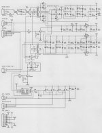
Hi all,
Project update,
Both power supply circuit boards have been designed now. I added a schematic diagram of the main power supply. This supply is used for the DAC itself, the second power supply is used for the tube output modules.
The current setup consumes about 44W, this could be slightly lowered by some optimizing.
The mains enters trough a PCB mount socket and passes a double mains-filter. Voltage selection for both 115Vac and 230Vac is provided by means of wire bridges. Transformer N3 also serves as stand-by power supply (system controller interface provides remote control functions). When in stand-by mode, relays K1...k4 are switched-off. D1 and D2 now provide the stand-by voltage and feed the on-board power supply (U2) for both the small microcontroller (U5) and the 5V relay's. When the system controller switches DACON "high", relays K1...K3 are powered and switch-on the main DAC supply (output's on J8). High efficiancy (ZTX653) transistors are used to get full 5V power for the relays.
Both U3 and U4 are pre-regulators for the 15V supplies, 5.1V zenerdiode's are used to obtain approx. 20V.
When the tube output is selected as well (tube or mixed mode), by bringing TUBON "high", microcontroller U5 now switches-on relay K4 that feeds the mains voltage to the tube power supply. It simultaneously output's a PWM 0.5 Hz sinewave signal. This signal is used to drive the 4 tube indicator LED's. R5 and C32 smoothen the signal, and JFET's T3...T6 make sure the maximum voltage is applied to the LED's. Due to the sinewave shape, the LED's start pulsating slowly indicating the differential tube output is being powered-up. After the LED's have pulsated 20 times, they remain on, indicating the differential tube output is now operational, simultaneously a switch signal is generated to connect the tube output to the main output.
When deselecting mixed mode or tube mode, the 4 LED's are slowly turned-off, relay K4 interrupts power to the differential tube output and the switch output disconnects the tube output signal from the main output.
Note, the microcontroller U5 is changed to a PIC12F629 now.
Attachments
- Home
- Source & Line
- Digital Line Level
- Building the ultimate NOS DAC using TDA1541A