I cleaned up my measuring system with another input device.
All measurements are made with 2 mA bias.
First 0 dB digital with 100 Ohm from DAC out to ground and no secondary load resistor (Pic. 100 Ohm Riv)
Next 0 dB digital with no Riv and 56K secondary load resistor . This value made the same level out of DAC @ 0dB digital.
If I reduce the digital level with 10-12 dB all harmonics disappear in the noise...
Almost no difference.
Then I measured 0 dB digital with 10K secondary load resistor and more gain after the DAC.
Notice the 3. harmonic is reduced as a result of the lover level at the output of the DAC.
I am not sure it is noticeable sound-wise I have not listened carefully for a prolonged period.
It is only the 2. and 3. harmonic that comes from the DAC/Preamp the rest are there even if I turn off the Dac.
If I reduce the digital level with 10-12 dB (turning up the preamp gain ) the 2. and 3. harmonic disappears .
Very similar to my findings re the 2nd and 3rd harmonics.
But my jury is still out as to whether your method or ECD's potential divider method is better, or indeed, if there is any measurable or audible difference between them.
I cleaned up my measuring system with another input device.
All measurements are made with 2 mA bias.
First 0 dB digital with 100 Ohm from DAC out to ground and no secondary load resistor (Pic. 100 Ohm Riv)
Next 0 dB digital with no Riv and 56K secondary load resistor . This value made the same level out of DAC @ 0dB digital.
If I reduce the digital level with 10-12 dB all harmonics disappear in the noise...
Almost no difference.
Then I measured 0 dB digital with 10K secondary load resistor and more gain after the DAC.
Notice the 3. harmonic is reduced as a result of the lover level at the output of the DAC.
I am not sure it is noticeable sound-wise I have not listened carefully for a prolonged period.
It is only the 2. and 3. harmonic that comes from the DAC/Preamp the rest are there even if I turn off the Dac.
If I reduce the digital level with 10-12 dB (turning up the preamp gain ) the 2. and 3. harmonic disappears .
Koldby,
You are using transformer with very low Rdc resistance of the primary coil. It is about 3.4ohm (from the datas). putting 100ohm in parallel resulting of 3.29ohm total. So it is no big difference.
Koldby,
You are using transformer with very low Rdc resistance of the primary coil. It is about 3.4ohm (from the datas). putting 100ohm in parallel resulting of 3.29ohm total. So it is no big difference.
It is the AC impedance that is important, not the DC resistance. There is no DC flowing through the trafos.
I think that it is not the case if we talking about IV conversion?
You can measure but direct at the Io of dac chip
a) Riv 100ohm II primary = 3.3ohm
b) just 3.3ohm Riv.
should be about the same value...
You can measure but direct at the Io of dac chip
a) Riv 100ohm II primary = 3.3ohm
b) just 3.3ohm Riv.
should be about the same value...
Oh yes it is.I think that it is not the case if we talking about IV conversion?
You can measure but direct at the Io of dac chip
a) Riv 100ohm II primary = 3.3ohm
b) just 3.3ohm Riv.
should be about the same value...
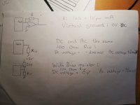
Take a look on the different ways to make I/V conversion.
In Pic 1 the first case shows a normal Opamp I/V conversion also known as virtual ground. The Opamp makes sure there is no (well almost no ) AC or DC at the Iout from the DAC. In the case of the TDA1541 you get 2V DC out of the Opamp with 1KOhm R and +/- 2V AC.
Second case passive I/V conversion: With 100 Ohm Riv:
You get -200 mV DC @ I out and this is overlayed with +/- 200mV AC.
So the Iout swings from 0 V to -400 mV and this causes elevated harmonic distortion from the TDA1541.
Third case passiv I/V with bias and 100 Ohm Riv:
The 2K5 to + 5V makes sure there is no DC current through the 100 Ohm Riv as it provides the 2 mA (5V/2K5 ) to the DAC.
Ac wise the 100 Ohm and 2K5 are in parallel, but this is insignificant so the AC @ Iout is +/-200 mV and this is much better for the TDA1541. Philips recomends no more than 25 mV (I guess RMS so P-P is 1,4 x 25 x 2 = +/- 70mV) for lowest distortion.
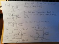
Now in pic 2 I show the different trafo cases:
First is a no go with the kind of trafos we are dealing with, as they are without air gab and therefore will magnetize the core, if exposed to DC current.
Second case:
To avoid DC through the trafos, there is a 2K5 resistor to +5V to make sure Iout is @ 0V DC. With a very high secondary loading of the trafo, Riv is again determining the AC voltage @ Iout = +/- 200 mV. With a 1:10 trafo 100K as load resistor will result in a 1K impedance in parallel with the 100Ohm Riv...
Third case:
Still a 2K5 to +5V to avoid DC through the Trafo.
Now in the case of 1:10 trafo if you use a 10 Kohm resistor as load for the trafo, this will be transformed to a 100 Ohm impedance @ Iout. As there is no DC at this point the DC resistance is of no importance here. AC wise the DC resistance is in fact in SERIES with the 100 Ohm transformed from the 10 KOhm load resistor. And it is part of the loss in the trafo..
Fourth and fifth cases:
This is what batteryman an I am working with presently.
In the fourth case the 2K5 bias resistor are not necessary form a DC flow in the trafos point of view, as the DC potential is the same (-200mV with 100 Ohm Riv) but we get into the same situation with the max swing (0 v to -400 mV) at both the Iout causing higher distortion.
The two Riv are acting as a 200 Ohm impedance between the two Iout resulting in +/- 400 mV from Iout+ to Iout -
The fifth case shows how I am doing it.
Here the 2K5 Ohm to +5V is necessary as there otherwise is no DC path for the 2mA bias required by the DAC (remember the DC potential is the same @ both + Iout and - Iout) .
Now if you load the secondary of the the trafo (1:10) with 20Kohm you get an AC impedance of 200 Ohm between the two Iout. Exactly the same as the fourth example.
I hope all this can help clean up the picture and remove misunderstandings.
Please do not be too harsh on me, if I have made some mistakes underways 😛
Attachments
I hope all this can help clean up the picture and remove misunderstandings.
Please do not be too harsh on me, if I have made some mistakes underways 😛
Yes its complete gibberish again! (not)

koldby, same can be achieved by connecting +5V through 1k25 to center tap. Magnetization due to currents flowing into the DAC will cancel each other.
koldby, same can be achieved by connecting +5V through 1k25 to center tap. Magnetization due to currents flowing into the DAC will cancel each other.
Sure if you have a center tap... My trafo hasen't
Sure if you have a center tap... My trafo hasen't
Mine do so I will try it in a few days and then also with the I/V resistors disconnected.
It is the AC impedance that is important, not the DC resistance. There is no DC flowing through the trafos.
It is the AC signal current through the DCR which performs the function of IV conversion. AC impedance is the same as DCR for a resistor. AC impedance of a transformer varies with frequency.
So you see what you write cannot be correct.
WRT comment re 25mV and datasheet, this is DC voltage compliance, 25mVDC, and not an vRMS value or anything else.
These are fundamental misunderstandings which have gone unchecked.
HK
Last edited:
So please tell me why the ac voltage across a trafo with 3,3 Ohm DC resistance is +/-200 mV with +/-2mA AC going through it? Ohms law is not valid any more?.It is the AC signal current through the DCR which performs the function of IV conversion. AC impedance is the same as DCR for a resistor. AC impedance of a transformer varies with frequency.
So you see what you write cannot be correct.
WRT comment re 25mV and datasheet, this is DC voltage compliance, 25mVDC, and not an vRMS value or anything else.
These are fundamental misunderstandings which have gone unchecked.
HK
Ac impedance of the primary of a transformer, within its working frequency and with a non reactive load on the secondary, is NOT varying with frequency. The impedance is the load resistance divided by the ratio between primary and secondary squared!
Concerning the compliance, you might be right, though 🙂
It is the AC signal current through the DCR which performs the function of IV conversion. AC impedance is the same as DCR for a resistor. AC impedance of a transformer varies with frequency.
So you see what you write cannot be correct.
WRT comment re 25mV and datasheet, this is DC voltage compliance, 25mVDC, and not an vRMS value or anything else.
These are fundamental misunderstandings which have gone unchecked.
HK
The trafos DC resistance is a few ohms but the centre tap (if present) needs to be fed the +2ma offset cancellation current from a low resistance source such as ECD's suggested circuit, not from a simple 2k resistor.
I think Sowter would have advised the I/V resistor could be dispensed with if it was not needed with either of their current output DAC I/V transformers but testing will probably shed light on the effect.
Last edited:
So please tell me why the ac voltage across a trafo with 3,3 Ohm DC resistance is +/-200 mV with +/-2mA AC going through it? Ohms law is not valid any more?.
Ac impedance of the primary of a transformer, within its working frequency and with a non reactive load on the secondary, is NOT varying with frequency. The impedance is the load resistance divided by the ratio between primary and secondary squared!
Concerning the compliance, you might be right, though 🙂
Yes you are right but I believe, this is only if the source resistance is very low. Whereas without an I/V resistor, its not?
Hi ceglar
Circuits meeting TDA1541A output compliance usually sound rather analytical.
Seems pure passive I/V can offer a more musical and involving sound.
In order to keep noise levels down it is best to generate highest possible signal amplitude while maintaining low THD.
Symmetrical voltage swing around 0V allows for maximum amplitude with low THD. This requires either a +2mA bias current or a suitable bias voltage that nulls DC on the TDA1541A output.
Tests showed that it is possible to squeeze out around 400mVpp this way while maintaining acceptable THD levels. This is not possible without using suitable bias current or bias voltage.
So now we have 400mVpp, loaded with unwanted RF noise, that needs to be amplified. Active amplification would cause troubles (RF noise). Adding a passive low pass filter in between would help.
But we could also use passive amplification plus RF filtering based on a step up transformer. Transformer with 1:10 transformation ratio would give us around 4Vpp. Output voltage can be lower in practical circuits due to losses.
The output impedance equals the input impedance times the transformation ratio squared. The output impedance would be much too high to drive loads directly.
The filtered 4Vpp output voltage could be buffered by a JFET and a small bias voltage could be subtracted in order to null DC on the JFET buffer output. This way there is no need for a coupling cap as the signal now swings between +2V and -2V.
I attached a circuit diagram of a practical circuit. 160R and 6R8 provide required bias voltage to get symmetrical swing around 0V. The I/V resistor of 100R connects between this bias voltage and the TDA1541A output. The TDA1541A output is also connected to the step up transformer. There will be approx. 400mVpp on the transformer primary with neglible DC offset voltage.
I used a cheap 1.5VA safety transformer with air gap (230V primary, 2 x 15V secondary) for testing. Transformation ratio equals 230 / 15 = 15.33. Depending on transformer properties a RC filter may be required across the transformer secondary to avoid ringing.
JFET source follower is used for buffering the step up transformer output signal. This way there is neglible load on the step up transformer. The 47R and 2K resistors provide a small negative bias voltage to null the DC voltage on the JFET buffer output so there is no need for a coupling cap. DC-offset on the JFET buffer output depends on JFET tolerances, and this can be corrected by changing the value of the 2K resistor or use a trimpot.
The circuit runs from the TDA1541A +5V and -5V supplies so no additional power supplies are required.
Enjoy.
My notions on the output compliance was wrong. Here are ECDesigns explanation of why I measure higher THD without the bias .
The trafos DC resistance is a few ohms but the centre tap (if present) needs to be fed the +2ma offset cancellation current from a low resistance source such as ECD's suggested circuit, not from a simple 2k resistor.
I think Sowter would have advised the I/V resistor could be dispensed with if it was not needed with either of their current output DAC I/V transformers but testing will probably shed light on the effect.
But Sowter does in fact do that:
DAC I/V CONVERSION OUTPUT TRANSFORMERS
Yes you are right but I believe, this is only if the source resistance is very low. Whereas without an I/V resistor, its not?
By source resistor do you mean secondary load resistance (the source resistance of the circuit connected to the secondary). If you disconnect the Riv on the primary side, you should place a resistor on the secondary side that is (with a 1:10 trafo ratio) 100 times the Riv you removed (10K secondary load is the same as a 100 Ohm Riv). Very low? not really...
And you should take into account the input impedance of the circuit that follows it. This is in parallel with the (10K) secondary resistor.
But Sowter does in fact do that:
DAC I/V CONVERSION OUTPUT TRANSFORMERS
Yes you are right. I didn't read far enough!
By source resistor do you mean secondary load resistance (the source resistance of the circuit connected to the secondary). If you disconnect the Riv on the primary side, you should place a resistor on the secondary side that is (with a 1:10 trafo ratio) 100 times the Riv you removed (10K secondary load is the same as a 100 Ohm Riv). Very low? not really...
And you should take into account the input impedance of the circuit that follows it. This is in parallel with the (10K) secondary resistor.
No I was wondering how the DAC output resistance might affect the sound?
(Doesn't a step up transformer need to be connected to a low impedance / high current source to produce a higher voltage at higher impedance /lower current output?)
No not necessary. DAC's with Iout are current output devices and they have high impedance.No I was wondering how the DAC output resistance might affect the sound?
(Doesn't a step up transformer need to be connected to a low impedance / high current source to produce a higher voltage at higher impedance /lower current output?)
- Home
- Source & Line
- Digital Line Level
- Building the ultimate NOS DAC using TDA1541A