Hi Eldam,
Thanks for the advice. In theory I understand the need to bypass coupling caps but in listening,
test, I just don't like the sound it produces in analog stage .
Cheers
Thanks for the advice. In theory I understand the need to bypass coupling caps but in listening,
test, I just don't like the sound it produces in analog stage .
Cheers
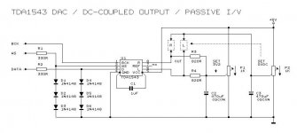
Hi maxlorenz,
I attached schematic of a TDA1543 DAC with DC-coupled outputs.
P1 is passive I/V resistor bias voltage (adjust to 3.2V).
P2 provides DC-coupled outputs (no coupling cap required). Adjust P2 for lowest DC offset on R and L outputs. This would give around 2.2V on the wiper of P2.
.
Hi -EC Designs-
I have a question regarding the DC coupled output you proposed, as I want to try my Dual-Mono TDA1543 with this feature...I understand P2 will set voltage on the "return" AKA "ground" connection of the output RCA, in order that the difference between "signal" and "return" are at 0VDC, but what about the next stage??? Won't the preamp see a (+) voltage on the "ground" also? 😕😕
I would appreciate if you could clarify this point.
Many thanks.
M.
Attachments
OK. I got it.
I got questions.
About Mosaic:
Do you find differences between well done 16/44 and "Hi Res" files on it?
It is not possible to make a 16/44 - 24/192 Mosaic SD player, without sound degradation?
About Dual-Mono:
What about introducing low value R between logic chips interconnections and also using ferrite beads on their power rails, to prevent interference?
The Dual-Mono DAC is indeed very involving and dynamic, as I said, and with silver wire jumpers for the digital section and OCC cables for interconnection and speakers (now trying DIY speaker cables, very slow to burn-in) I achieved very open sound, which is not what we usualy expect with the veteran.
This is the best poor-man's DAC that I tried so far. 😎
The sounds jumps at you in the fff passages, but it is not always upfront like other DACs are as the soundstage has proper depth, plenty of it...it is very hard to go to work... 🙁
Now listening Mahler's fift; very enjoyable, though I'm not a fan of Mahler.
Best wishes,
M.
Hi Max Mahler 5 which Orchestra Conductor ??
Onno Onnosr
Hi dear 🙂
Good question...I am not sure what version it was, as I usually erase all "superfluous" data on the title when writing the SD card. It was either Sir John Barbirolli's or Leonard Berstein's, probably the later... 😕
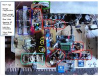
I attach a picture about the present state of my SD card player with dual mono TDA1543 DAC section, with lots of Vregs. The adddition of John's shunt regulators to the SD player's clock and main receiver chip made a big improvement and took out some "digital" sound that was still there. 😎
I hope I will good news soon 😉
Cheers,
M.
PS: Anybody had the chance of listening the new Mosaic???
Good question...I am not sure what version it was, as I usually erase all "superfluous" data on the title when writing the SD card. It was either Sir John Barbirolli's or Leonard Berstein's, probably the later... 😕
I attach a picture about the present state of my SD card player with dual mono TDA1543 DAC section, with lots of Vregs. The adddition of John's shunt regulators to the SD player's clock and main receiver chip made a big improvement and took out some "digital" sound that was still there. 😎
I hope I will good news soon 😉
Cheers,
M.
PS: Anybody had the chance of listening the new Mosaic???
Attachments
Hi Max
Shunts to main receiver chip !!!!. Do you mean the dac ?
Btw where can I find John's shunt schematics
Thanks
Shunts to main receiver chip !!!!. Do you mean the dac ?
Btw where can I find John's shunt schematics
Thanks
Hi Max
Shunts to main receiver chip !!!!.
Thanks
I think it's the main receiver chip. Sorry, it is covered by my magic varnish so I can't read what's writen.
I attach the schematics. Vout depends on Vin and R3/R4, or something like that. I added a pre-reg to be on target on some spots.
Cheers,
M.
Attachments
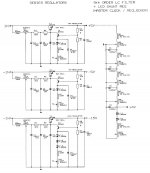
The upper schematic is the (+) shunt regulator but you have to modifye the R3/R4 or use a pre-reg, given your Vin and your desired Vout, if you don't have the chance of getting the perfect Vout already.
The +4V from LC filter can be used as a very silent Voltage bias for the TDA1543 DAC chips. Use that and a high quality wirewound R for I/V and you will have a worthy DAC.
I took the liberty of compounding a schematic of different schematics from -EC- and that is what I am using now. This is not "-EC- approuved" yet, guys.
Attachments
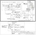
Sorry Max am a little confused at the output after the I/V resistor. I see a 5v vcc supply with
1k VR that connects back to output of both Dac with a 470uf shunt cap. Exactly what does this do.
Thanks again
1k VR that connects back to output of both Dac with a 470uf shunt cap. Exactly what does this do.
Thanks again
Apologies Max studied the schematics again. Ok I understand it's purpose now.
Btw I read threads that many are running the 1543 at almost 8v. Do you find any
difference in sound quality ?
Thanks again
Btw I read threads that many are running the 1543 at almost 8v. Do you find any
difference in sound quality ?
Thanks again
Sorry, I should have explained that before. That circuit allows for either powering both, the DAC chips and the V bias from the same quality V reg, using P1 to set V bias, OR using a quality reference as the LC circuit (you can omit P and C if you like) shown above to set V bias independently of the V reg for the DAC chips. For setting V bias you have to consider the value of I/V R. In this dual mono setting I out is doubled so for a 500R I/V that I use, V out is 0.0046*500= 2.3V. I set it to 4.2V to be safe...other idea that I have not tested yet is using only Pin 8 as output, in which case Vout is halved...
I have used VCC as low as 3.8 and I think I prefer lower (5.3 to 3.8V) power as it sounds cleaner. The chips are already warm sounding so the added warmth that high VCC gives is not needed in my view, wastes heat and may add distortion.
Maybe -EC- measured that time ago; I'm not sure...
Note that the circuit allows for AC coupling (return to ground) or DC coupling with P2, which I have not tested yet... 😱
Best wishes,
M.
I have used VCC as low as 3.8 and I think I prefer lower (5.3 to 3.8V) power as it sounds cleaner. The chips are already warm sounding so the added warmth that high VCC gives is not needed in my view, wastes heat and may add distortion.
...
Someone did a graph showing that you need Vcc =~ 7.5V to get ... full 16 bit DAC resolution, or adequate noise performance or full output swing for 16bit or ... something. I.E. not 5 V.
But maybe this doesn't apply to you in balanced mode ...
Cheers,
Jeff
Last edited:
Someone did a graph showing that you need Vcc =~ 7.5V to get ... full 16 bit DAC resolution, or adequate noise performance or full output swing for 16bit or ... something. I.E. not 5 V.
But maybe this doesn't apply to you in balanced mode ...
Cheers,
Jeff
Thanks for your input. Maybe that was reffering to an 8 or more DAC tower?
Anyway, it seems that a batch of 100 DACs will have only a few that will deliver the promised resolution and noise figures that the maker (with small "m") stated. There are some mates that have the equipment to select the best...otherwise they can be selected by ear but it is not easy, even more if you have to select two...
Some years ago I got rid of my audiophilia nervosa and now it seems I am happy with 14bits, provided there is a lot of dynamics, punch and palpability of images, which this DAC provides. 🙂
Even dirty and raw, the long term listening is still fun, compared to the clean, resolving and polite cheap Sabre DACs that I own, which are rather boring in the long term.
This dual-mono DAC is not balanced (the DI4M was balanced to single ended using discrete differential amplifier) though I plan to use direct out to a input TX, sort of balanced...
Cheers,
M.
...
Even dirty and raw, the long term listening is still fun, compared to the clean, resolving and polite cheap Sabre DACs that I own, which are rather boring in the long term.
This dual-mono DAC is not balanced (the DI4M was balanced to single ended using discrete differential amplifier) though I plan to use direct out to a input TX, sort of balanced...
....
1.o = 1.4 Vrms, !
1 Vrms.
...
1.83 Vprms
No, it was firm!
Last edited:
Sorry. I did not get it.
I could test the sound with higher VCC when I reconnect the SuperTeddyReg again. 😉
M.
I could test the sound with higher VCC when I reconnect the SuperTeddyReg again. 😉
M.
Hi maxlorenz,
The DAC has galvanically insulated supply and the next stage has a galvanically insulated supply. GND (0V) of the DAC is -NOT- connected to GND (0V) of the next stage. The GND of the next stage is connected to RGND (reference ground) of the DAC.
So basically all circuits are connected to GND as usual, except the DAC local "0V GND" is a negative voltage with respect to this GND.
Just imagine your next stage is a multimeter with its own 9V battery supply. The GND of the multimeter (black wire) is connected to DAC reference voltage (say +2V) and the input (red wire) is connected to the DAC output that also has +2V DC (all measured with respect to DAC true GND). Then the multimeter DC voltage reading would be zero.
This approach is different from using a coupling cap. Even the best coupling cap will add distortion and causes loss of resolution.
The output signal now connects directly to the next stage (DC-coupled). GND return path connects to a power supply with very low output impedance that can be bypassed with a low ohmic resistor. When a coupling cap would be bypassed with a low ohmic resistor its degrading will be greatly reduced, but then it looses its function of blocking DC … The RGND approach does not have this problem.
Similar to a coupling cap, every active circuit will also introduce distortion and loss of resolution. The more active circuits / components in the signal path, the worse it will get.
Hi -EC Designs-
I have a question regarding the DC coupled output you proposed, as I want to try my Dual-Mono TDA1543 with this feature...I understand P2 will set voltage on the "return" AKA "ground" connection of the output RCA, in order that the difference between "signal" and "return" are at 0VDC, but what about the next stage??? Won't the preamp see a (+) voltage on the "ground" also? 
The DAC has galvanically insulated supply and the next stage has a galvanically insulated supply. GND (0V) of the DAC is -NOT- connected to GND (0V) of the next stage. The GND of the next stage is connected to RGND (reference ground) of the DAC.
So basically all circuits are connected to GND as usual, except the DAC local "0V GND" is a negative voltage with respect to this GND.
Just imagine your next stage is a multimeter with its own 9V battery supply. The GND of the multimeter (black wire) is connected to DAC reference voltage (say +2V) and the input (red wire) is connected to the DAC output that also has +2V DC (all measured with respect to DAC true GND). Then the multimeter DC voltage reading would be zero.
This approach is different from using a coupling cap. Even the best coupling cap will add distortion and causes loss of resolution.
The output signal now connects directly to the next stage (DC-coupled). GND return path connects to a power supply with very low output impedance that can be bypassed with a low ohmic resistor. When a coupling cap would be bypassed with a low ohmic resistor its degrading will be greatly reduced, but then it looses its function of blocking DC … The RGND approach does not have this problem.
Similar to a coupling cap, every active circuit will also introduce distortion and loss of resolution. The more active circuits / components in the signal path, the worse it will get.
Hi maxlorenz,
The DAC has galvanically insulated supply and the next stage has a galvanically insulated supply. GND (0V) of the DAC is -NOT- connected to GND (0V) of the next stage. The GND of the next stage is connected to RGND (reference ground) of the DAC.
Thank you, dear -EC-, for the detailed explanation.
So, for me, the best option is to run the output of the DAC through my high quality TVC...or build a DC coupled preamp/buffer stage with floating supply.
Appart, I visit your site regularly and it has not been updated 😡 😀
How can I order the Mosaic?
(Anything to do with the Mosaic Law?)
https://archive.org/stream/hebraictonguere00oligoog#page/n521/mode/2up
Thank you again for your constant tuition 🙂
Best wishes,
M.
PS: please check your inbox.
This is my first post here, so hello everybody 🙂
Some time ago, I salvaged a TDA1541 chip from an old cd player. Since then, I've seen many different projects and kits, but so far, all of them were based on PCBs which you couldn't make at home.
So, forgive me for not reading everything, but 546 pages is a little too much for me 😉 Is there a complete, working DAC project with good description, which I could build at home (etch my own PCB) ? I will appreciate any help 🙂
Could be NOS or not.
- Home
- Source & Line
- Digital Line Level
- Building the ultimate NOS DAC using TDA1541A