Thanks...AHAHA so cute shematic Esgigt 🙂
miss the passive low pass filter before the amp...
I intentionally omitted the LPF.... just to keep it VERY simple. True, I ought have mentioned it..
PS: I abused MS-PP for the drawing... LOL
Last edited:
But I'm very interested by the concept with the link between the gnd at the output of the resistor and the TDA you draw in the shematic... some will say with a continous gnd plane : current will find its way !
I liked the old parts of this thread where John was developping an all in one concept around the DAC, the pre and amp to drive the speakers ! Risky in a marketing side but brilliant in a pragmatic side for the Sound quality result....Maybe a good buffer with volume and impedance matching (is it the name for a pre ?) is enough and good for a all in one DAC 😉.... Yes this story of volume pot is important.... let swap our pre, most of the time for people like me we have no sota pre and they just are usefull for sources swapping !
I liked the old parts of this thread where John was developping an all in one concept around the DAC, the pre and amp to drive the speakers ! Risky in a marketing side but brilliant in a pragmatic side for the Sound quality result....Maybe a good buffer with volume and impedance matching (is it the name for a pre ?) is enough and good for a all in one DAC 😉.... Yes this story of volume pot is important.... let swap our pre, most of the time for people like me we have no sota pre and they just are usefull for sources swapping !
I tried last week free running DEM with 2 x 12K to -18V
(820pF remain in place)
But on TDA1540D chip, and it improved a sound
voltage measured on the dem pins was WO R to /18V something about -13.5V
and when 2 resistors in circuit, moved a little bit to -14.5 cca, each pin
measired on dacs playing... 🙂
I will measure with the scope dem signals, in factory proposed circuit WO dem R it was just like it should be...
.
So it is working with TDA1540 too.
.
I am using 5 ohm Riv to stay within 10mV off set for this dac. 2mA JFET current injection at Iout pin,
JFET SE gain stage after followed by the JFET buffer. Just simple way to try
.
Sys was MacMiniI7-Amanero-CPLD-TDA1540D (dual Mono)
played in nos mode to 192KHz and passing even to 38xKHz but with little cracking.
maybe because the longer signal lines... this dac has 12Mbs (more than TDA1541A) so if I am not wrong the MCK can be up to around 12MHz
I didnt believe how sweet and good this old chip is. 🙂
no digitalis, Ihave to readljust my speakers crossover to give more gain to the upper horns. Somehow TDA1540D reduce beaming of the EHP-HYP horns, which Im intend to exchange to WG or pure EXP...
.
One thing could be of the interest for TDA1541A funclub. The temperature.
Once I have some CD players with the TDA1540. And the chips are somehow get more than warm?
in my simple set up the chips are just slight warm (maybe because of the open experimental housing)
But I made experiment and I mount each TDA1540D on the bigger heatsinks.
temperature decreased additionally, and I think that the sound is more clear and even with less distortion?
.
So I recommend that for the TDA1541A too - to mount on the heatsink - bigger.
Last edited:
I put trivial ceramic dem decoupling caps at tda1540, just to make it working...
But which type of C is better for this pins?
Thanks. 🙂
But which type of C is better for this pins?
Thanks. 🙂
Hi Zoran, do you mean we have to apply heavier heat sinks ? What about the temperature required /or suggested/?One thing could be of the interest for TDA1541A funclub. The temperature.
Cheers,
The temperature of My ceramic TDA1540D is about or little bit under body temp.
it is hard to tell (I will try to measure) without any heatsink and in open housing.
.
I put all the elements at one and chip to another side of the board, so I have all space to aproach to heatsink. I didnt put the thermo white fluid for better heat conducting, (dont want to poluting chip from the top - yet...)
.
As the temperature lower the sound is clearer, it is better to be under room temp but there is hard to acheive, so please tru with just possible to mount as bigger as it could heatsink.
.
You will spot the diferents 🙂
And I am pretty shure that is can addressed to TDA1541A chip too.
for instance it will be nice to have the heatsink like Yours BUT with tha same flat area like on the area to chip top comtact, then You can mount bigger heatsink over?
I have 1 Q please
IS the simple 2 x R circuit to DEM pins and -V (higher) adding OR substracting amount of current from/to existing inside circuit in dac chips?
IS the simple 2 x R circuit to DEM pins and -V (higher) adding OR substracting amount of current from/to existing inside circuit in dac chips?
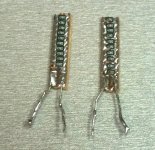
I made some quick Riv from smd Rs, there are 10 x 47R in parallel for 4,7R Riv
first version, now I am using (red one in the pic) 20 x 100R for 5R
booth version with simple jfet BF245 2mS set current injection.
.
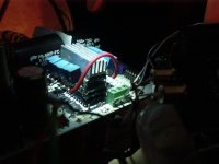
You can see the heat sink on the top of the dac chip.
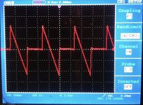
and factory just 820pF simple ceramic dem cap signal at dem pins measured.
🙂
first version, now I am using (red one in the pic) 20 x 100R for 5R
booth version with simple jfet BF245 2mS set current injection.
.
You can see the heat sink on the top of the dac chip.
and factory just 820pF simple ceramic dem cap signal at dem pins measured.
🙂
Attachments
Thanks, I got it and will try asap !for instance it will be nice to have the heatsink like Yours BUT with tha same flat area like on the area to chip top comtact, then You can mount bigger heatsink over?
The latest projects are based on passive I/V conversion:
50 Ohm I/V resistor (between TDA1541A output and GND)
Hi John,
Which is better solution by your opinion - to solder the I/V 50 ohms res straight on the output pin of the TDA or to go with the current to the tube grid and convert the signal there ?
Thanks,
Ignat
Zoran,
How are the TDA1540Ds feeded ? Via the SA7030 or Ian's device ?
Did you try the last DEM clock value John uses with the TDA1541 ?
How are the TDA1540Ds feeded ? Via the SA7030 or Ian's device ?
Did you try the last DEM clock value John uses with the TDA1541 ?
Heatsink on TDA1541A
Actually I already discovered its benefits:
http://www.diyaudio.com/forums/digital-line-level/160265-copper-tape-atop-ics-2.html#post2069735
http://www.diyaudio.com/forums/digi...e-nos-dac-using-tda1541a-360.html#post2469333
Simple and effective mod!
Actually I already discovered its benefits:
http://www.diyaudio.com/forums/digital-line-level/160265-copper-tape-atop-ics-2.html#post2069735
http://www.diyaudio.com/forums/digi...e-nos-dac-using-tda1541a-360.html#post2469333
Simple and effective mod!
Hi John,
Which is better solution by your opinion - to solder the I/V 50 ohms res straight on the output pin of the TDA or to go with the current to the tube grid and convert the signal there ?
Thanks,
Ignat
IMHO the resistor should go near the dac chip; AND to overcome an open antenna, add two stoppers of say 100 ohm:
- a stopper resistor at the connection attached to the Riv of 50 ohm
- and also one at the tube at the other end of the connection.
You can put a damping capacitor on the 50 ohm if you like. Say 1 nF. Some (like I) do it complicated but that is up to you. It depends on the output: with a tube like ECC88 the need is less for a HF cut - again imho.
Hi Eldam 🙂
I tryed also to put SAA7030 digital filter before the dac chip, but somehow I dont like it?
Still it is not the same sound like in all players where theese chips working together, but I prefer for the moment NOS mode. first because I can play higher sampling rates almost to the 38XKHz. I didnt try Ians interface still, but I will be make this test soon, I have boards, just didnt have time to check.
I put free running dem EC style, but with 820pF and 2 x 12K @-18V for TDA1540D chip.
for the first try i put little bit higher values? And keep the 820pF just to remain dem Fo, (like EC did for 470pF TDA1541A)
.
Last edited:
I tryed also my version of National high gain jfet stage, and working good
but I refer back to litle bit less gain, classic JFET stage followed by JFET simple buffer
with Riv=5R, and Iinject=2mA
SE topology, NON-complementary devices, off-course 🙂
(I think I can never go back to complementary devices again...
but I refer back to litle bit less gain, classic JFET stage followed by JFET simple buffer
with Riv=5R, and Iinject=2mA
SE topology, NON-complementary devices, off-course 🙂
(I think I can never go back to complementary devices again...
I think that Current injection has to be close to the Iout pin,
But Riv can be just @ the input of gain stage?
.
(off course not 100m away from dac chip,)
🙂
I did it 5-6cm from TDA1540 dac.
But Riv can be just @ the input of gain stage?
.
(off course not 100m away from dac chip,)
🙂
I did it 5-6cm from TDA1540 dac.
Hi ceglar
Circuits meeting TDA1541A output compliance usually sound rather analytical.
Seems pure passive I/V can offer a more musical and involving sound.
In order to keep noise levels down it is best to generate highest possible signal amplitude while maintaining low THD.
Symmetrical voltage swing around 0V allows for maximum amplitude with low THD. This requires either a +2mA bias current or a suitable bias voltage that nulls DC on the TDA1541A output.
Tests showed that it is possible to squeeze out around 400mVpp this way while maintaining acceptable THD levels. This is not possible without using suitable bias current or bias voltage.
So now we have 400mVpp, loaded with unwanted RF noise, that needs to be amplified. Active amplification would cause troubles (RF noise). Adding a passive low pass filter in between would help.
But we could also use passive amplification plus RF filtering based on a step up transformer. Transformer with 1:10 transformation ratio would give us around 4Vpp. Output voltage can be lower in practical circuits due to losses.
The output impedance equals the input impedance times the transformation ratio squared. The output impedance would be much too high to drive loads directly.
The filtered 4Vpp output voltage could be buffered by a JFET and a small bias voltage could be subtracted in order to null DC on the JFET buffer output. This way there is no need for a coupling cap as the signal now swings between +2V and -2V.
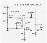
I attached a circuit diagram of a practical circuit. 160R and 6R8 provide required bias voltage to get symmetrical swing around 0V. The I/V resistor of 100R connects between this bias voltage and the TDA1541A output. The TDA1541A output is also connected to the step up transformer. There will be approx. 400mVpp on the transformer primary with neglible DC offset voltage.
I used a cheap 1.5VA safety transformer with air gap (230V primary, 2 x 15V secondary) for testing. Transformation ratio equals 230 / 15 = 15.33. Depending on transformer properties a RC filter may be required across the transformer secondary to avoid ringing.
JFET source follower is used for buffering the step up transformer output signal. This way there is neglible load on the step up transformer. The 47R and 2K resistors provide a small negative bias voltage to null the DC voltage on the JFET buffer output so there is no need for a coupling cap. DC-offset on the JFET buffer output depends on JFET tolerances, and this can be corrected by changing the value of the 2K resistor or use a trimpot.
The circuit runs from the TDA1541A +5V and -5V supplies so no additional power supplies are required.
Enjoy.
You're ok with exceeding output voltage compliance with 1541A as per 50R I/V?
Circuits meeting TDA1541A output compliance usually sound rather analytical.
Seems pure passive I/V can offer a more musical and involving sound.
In order to keep noise levels down it is best to generate highest possible signal amplitude while maintaining low THD.
Symmetrical voltage swing around 0V allows for maximum amplitude with low THD. This requires either a +2mA bias current or a suitable bias voltage that nulls DC on the TDA1541A output.
Tests showed that it is possible to squeeze out around 400mVpp this way while maintaining acceptable THD levels. This is not possible without using suitable bias current or bias voltage.
So now we have 400mVpp, loaded with unwanted RF noise, that needs to be amplified. Active amplification would cause troubles (RF noise). Adding a passive low pass filter in between would help.
But we could also use passive amplification plus RF filtering based on a step up transformer. Transformer with 1:10 transformation ratio would give us around 4Vpp. Output voltage can be lower in practical circuits due to losses.
The output impedance equals the input impedance times the transformation ratio squared. The output impedance would be much too high to drive loads directly.
The filtered 4Vpp output voltage could be buffered by a JFET and a small bias voltage could be subtracted in order to null DC on the JFET buffer output. This way there is no need for a coupling cap as the signal now swings between +2V and -2V.
I attached a circuit diagram of a practical circuit. 160R and 6R8 provide required bias voltage to get symmetrical swing around 0V. The I/V resistor of 100R connects between this bias voltage and the TDA1541A output. The TDA1541A output is also connected to the step up transformer. There will be approx. 400mVpp on the transformer primary with neglible DC offset voltage.
I used a cheap 1.5VA safety transformer with air gap (230V primary, 2 x 15V secondary) for testing. Transformation ratio equals 230 / 15 = 15.33. Depending on transformer properties a RC filter may be required across the transformer secondary to avoid ringing.
JFET source follower is used for buffering the step up transformer output signal. This way there is neglible load on the step up transformer. The 47R and 2K resistors provide a small negative bias voltage to null the DC voltage on the JFET buffer output so there is no need for a coupling cap. DC-offset on the JFET buffer output depends on JFET tolerances, and this can be corrected by changing the value of the 2K resistor or use a trimpot.
The circuit runs from the TDA1541A +5V and -5V supplies so no additional power supplies are required.
Enjoy.
Attachments
IMHO the resistor should go near the dac chip; AND to overcome an open antenna, add two stoppers of say 100 ohm:
Note the DAC output is well into the MHz (rising edges) so this can provide coupling throughout the dac chassis.
- a stopper resistor at the connection attached to the Riv of 50 ohm
- and also one at the tube at the other end of the connection.
You can put a damping capacitor on the 50 ohm if you like. Say 1 nF. Some (like I) do it complicated but that is up to you. It depends on the output: with a tube like ECC88 the need is less for a HF cut - again imho.
Thanks for your suggestions. I will try the STOPPERS but excuse my ignorance I am afraid it will change the value of the I/V res if not big value /in parallel/ ??
Regards,
Ignat
- Home
- Source & Line
- Digital Line Level
- Building the ultimate NOS DAC using TDA1541A