Hi JOSI1,
SD8-transport, 240mm x 90mm x 9mm.
TDA1541A-MK10, 120mm x 50mm x 9mm.
TDA1543-MK10, 120mm x 50mm x 9mm.
Stepped shunt volume control, 120mm x 50mm x 9mm.
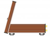
SD8-transport, DAC and volume control are housed in a tilted vertical panel measuring 160mm x 260mm x 15mm. It's mounted to a base measuring 180mm x 180mm x 40mm containing power supplies and connectors.
I attached some sketches.
Housing consists of sandwich construction of aluminum sheets and wood.
The shunt regulators have different schematic and they are no longer powered through CCS.
I now use passive balanced 10th order RC filters between rectifier bridges and shunts. The resistors in the filters also limit the current for the connected shunt so no additional current limiting resistors are required.
I use RF JFETs (BF862). The gate connects to the wiper of a 1K trimmer, one side of the trimmer connects to GND, the other to -15V through 15K series resistor. Trimmer is adjusted for approx. 0 ... -20mV DC on the TDA1541A output. Each JFET has a separate trimmer plus 15K series resistor.
What are the board dimensions of the SD8-transport, TDA1541A-MK10 and Volume Control.
SD8-transport, 240mm x 90mm x 9mm.
TDA1541A-MK10, 120mm x 50mm x 9mm.
TDA1543-MK10, 120mm x 50mm x 9mm.
Stepped shunt volume control, 120mm x 50mm x 9mm.
Can you give some informatons about the mechanical concept of the SD8-Player.
SD8-transport, DAC and volume control are housed in a tilted vertical panel measuring 160mm x 260mm x 15mm. It's mounted to a base measuring 180mm x 180mm x 40mm containing power supplies and connectors.
I attached some sketches.
Housing consists of sandwich construction of aluminum sheets and wood.
The MK10 board has 4 embedded Shunt regulators. Do reuse the concept/schematic described in post #4175 (cap multiplier / parallel constant current sources on each leg, shunt regulator) or is this concept already out-dated.
The shunt regulators have different schematic and they are no longer powered through CCS.
I now use passive balanced 10th order RC filters between rectifier bridges and shunts. The resistors in the filters also limit the current for the connected shunt so no additional current limiting resistors are required.
For the MK10 you are using a new DAC output stage based on SMD JFETs as current buffer.
Could you please tell what JFET you use or post a schematic?
I use RF JFETs (BF862). The gate connects to the wiper of a 1K trimmer, one side of the trimmer connects to GND, the other to -15V through 15K series resistor. Trimmer is adjusted for approx. 0 ... -20mV DC on the TDA1541A output. Each JFET has a separate trimmer plus 15K series resistor.
Attachments
Hello John,
thank you for your informations. Concerning the current buffer
I'm not sure if the following components from former designs
are still necessary:
Resistor for bias current: 2M2 remains
C=1uF from wiper to GND ??
resistor between wiper and Gate of FET ??
C=150pF from Source to GND ??
thank you for your informations. Concerning the current buffer
I'm not sure if the following components from former designs
are still necessary:
Resistor for bias current: 2M2 remains
C=1uF from wiper to GND ??
resistor between wiper and Gate of FET ??
C=150pF from Source to GND ??
Hi JOSI1,
2M2 resistor remains, it prevents BF862 from going out of conduction when TDA1541A output current approaches zero).
1uF capacitor is now removed.
No resistor between trimmer and JFET, 1K trimmer now serves as gate stopper.
150pF capacitor is now removed.
Resistor for bias current: 2M2 remains
2M2 resistor remains, it prevents BF862 from going out of conduction when TDA1541A output current approaches zero).
C=1uF from wiper to GND ??
1uF capacitor is now removed.
resistor between wiper and Gate of FET ??
No resistor between trimmer and JFET, 1K trimmer now serves as gate stopper.
C=150pF from Source to GND ??
150pF capacitor is now removed.
Hi JOSI1,
The shunt regulators have different schematic and they are no longer powered through CCS.
I now use passive balanced 10th order RC filters between rectifier bridges and shunts. The resistors in the filters also limit the current for the connected shunt so no additional current limiting resistors are required.
.
Hello John,
is it possible to post a schematic of the new shunt regulator and the balanced RC filter?
MK8 concept schematics.
I attached TDA1541A-MK8 concept schematics.
On the top there are 4 common mode voltage regulators for +5V, -5V, -15V, and +5V. They consist of cascaded filtered buffered zener diode regulators.
This works as follows, T1 and D5 form a 10V - 1.2V = 8.8V pre regulator. This pre regulator is placed in the ground reference line. T5 and D1 form a 6.2V - 1.2V = 5V post regulator that is referenced to the 8.8V GND reference provided by the pre regulator. R7 and C23 filter the zener diode noise.
The 5V post regulator is placed after the 8.8V pre regulator and re-stabilizes it to +5V. The output of the 8.8V pre regulator serves as ground reference. The output of the post regulator is decoupled to GND by a 1uF SMD film cap (C11).
The negative common mode voltage regulators function similar. The -15V regulator has a -18.8V pre regulator and a -15V post regulator.
Note that all common mode regulators have separate plus and minus inputs that are connected to the main power supply using twisted pairs. The main power supply contains rectifiers, smoothing caps and common mode capacitance multipliers.
John, I have built the regulators of post 4008. The -15V rail seems ok, but the + and - 5V rails are + and - 6.5V. If I'm not mistaken, this is outside the tolerance for the tda1541a, isn't it? Is the schematic of post 4008 correct?
Dear ec
Excuse me, but
I don't see anybody talking about 24 bit systems.
The 1541A still got 16 bit theoretical.
To the facts:
Your argumentation is again totally wrong.
Edl of typical 0.5 LSB sounds very nice but it isn't.
It is true that 0.5 LSB can be ignored in a 16 bit system at full scale.
Unfortunately the Edl has not much to do with full scale.
It is specially related to low level signals for a good reason.
At -60 dB the effective DAC resolution is reduced to 9-10 bits and things look very different.
0.5 LSB is blown up and becomes an unacceptable value if your goal is a high end system.
Calculation for 1 LSB change in a 9 bit system:
1,000,000 / 512 = 1953 cm = 0,02 km on a distance of 10 kilometer.
Remember that audio uses a logaritmic scale, because of the extremely high dynamic range of the ear.
Philips quotes -42 dB distortion for the 1541A at -60 dB which is not very impressive.
I got clearly better results with a few lucky 1541A chips, but still far from the optimum.
Edl must be at least reduced to < 0.02 LSB.
The "right" DAC chips allow to adjust Edl to zero.
From a Burr Brown DAC datasheet:
"DLE is important in audio applications because excessive DLE at Bipolar Zero can result in audible crossover distortion for low level output signals."
For a critical listener, DLE does not need to be excessive to be audible.
If you playback a full scale signal, perhaps.

You will understand that I feel myself obligated to make corrections when I see that dangerous halfknowledge is spread in the forum.
Hi triode_al,
That's bernhard's personal opinion.
Excuse me, but
I rely on facts like Philips datasheet specs and publications that specify Edl of typical 0.5 LSB and MSB change glitch of 0.25 LSB for TDA1541A. These were carried out using a decent lab measurement setup. Poor TDA1541A application and / or measurement setup can lead to different measurement results and that's probably what happened here.
We talk about LSBs and 16 ... 24 bit resolution and how important it is to gete every last bit.
Imagine we visualize bit resolution by translating DAC full-scale output signal to say a distance of 10 kilometer or 1,000,000cm. Then a LSB change on a 16 bit system would represent 1,000,000 / 65,536 = 15cm on a distance of 10 kilometer.
I don't see anybody talking about 24 bit systems.
The 1541A still got 16 bit theoretical.
To the facts:
Your argumentation is again totally wrong.
Edl of typical 0.5 LSB sounds very nice but it isn't.
It is true that 0.5 LSB can be ignored in a 16 bit system at full scale.
Unfortunately the Edl has not much to do with full scale.
It is specially related to low level signals for a good reason.
At -60 dB the effective DAC resolution is reduced to 9-10 bits and things look very different.
0.5 LSB is blown up and becomes an unacceptable value if your goal is a high end system.
Calculation for 1 LSB change in a 9 bit system:
1,000,000 / 512 = 1953 cm = 0,02 km on a distance of 10 kilometer.
Remember that audio uses a logaritmic scale, because of the extremely high dynamic range of the ear.
Philips quotes -42 dB distortion for the 1541A at -60 dB which is not very impressive.
I got clearly better results with a few lucky 1541A chips, but still far from the optimum.
Edl must be at least reduced to < 0.02 LSB.
The "right" DAC chips allow to adjust Edl to zero.
From a Burr Brown DAC datasheet:
"DLE is important in audio applications because excessive DLE at Bipolar Zero can result in audible crossover distortion for low level output signals."
For a critical listener, DLE does not need to be excessive to be audible.
With these high to extreme resolutions, the limits of audio equipment will be the dominating factor, not DAC bit resolution.
If you playback a full scale signal, perhaps.
You will understand that I feel myself obligated to make corrections when I see that dangerous halfknowledge is spread in the forum.
Last edited:
Bernhard, you may or may not be right. But please, this is a thread about TDA1541A, not the right plase for your crusade against this chip. Open your thread and put your measurements and theories about the "right" chip there.
Bernhard, you may or may not be right. But please, this is a thread about TDA1541A, not the right plase for your crusade against this chip. Open your thread and put your measurements and theories about the "right" chip there.
My posting was mostly about DA conversion theory in general.
Pardon me for mentioning a "right" chip.
If you not wish to read my postings, you can add me to your ignore list.
User CP --> Settings and options --> Edit ignore list.
Maybe Bernhard is "hard" in his writings, but even If I don't agree with a couple of things with him, I like other points of view, so I think it's good for all. With think like this one can think in another ways and try another theories or experiments......
Completely agree, and i like to read these statements.
But in my view, these (yes, i mean several) posts which are telling us and especially to the thread opener, that his main and central design decision (i.e. using TDA1541A) is wrong do not belong here.
In my eyes it's simply impolite and does not help the discussion about his development, which is about implementing this chip and not another one. It belongs elsewhere.
As no one would burst into the Pass Forum, eg. the BA-2 thread, and tell everyone and Nelson Pass that MOS-FET's in the output stage are a bad thing.
But in my view, these (yes, i mean several) posts which are telling us and especially to the thread opener, that his main and central design decision (i.e. using TDA1541A) is wrong...
Because of the thread title.
Building the ultimate NOS DAC using TDA1541A
At least three essential limitations of the TDA1541A raise serious concerns and the question if the goal could be achieved.
More appropriate would have been:
Building the ultimate TDA1541A DAC using NOS
In my eyes it's simply impolite and does not help the discussion about his development, which is about implementing this chip and not another one. It belongs elsewhere.
You say it yourself: The goal and core theme is clearly "Building the ultimate NOS DAC"
The main and central design decision is the choice of the DAC chip TDA1541A.
- Why the TDA1541A? it uses current sources based on dynamic element matching instead of resistor networks. The current sources are externally decoupled so they produce clean signals. Furthermore a smart design elliminates signal transients all together.
Tips or suggestions from you all are highly appreciated
"ultimate" is a very big claim. As this is a discussion forum, not a sweet talk-blindly believing everything-place, criticism about the primary design choice must be expected. If the criticism is ignored or responded with false/wrong/weak arguments, the criticism will continue.
As no one would burst into the Pass Forum, eg. the BA-2 thread, and tell everyone and Nelson Pass that MOS-FET's in the output stage are a bad thing.
I'm not aware of a Nelson Pass thread titled "Building the ultimate classA amplifier using MOSFET output stage."
Last edited:
Dear Bernhard,
I think the problem might be related with reading comprehension... 😉
"Building the ultimate NOS DAC using TDA1541A"
Means to me: "creating the best DAC that can be made with the TDA1541 chip".
(which might also be the best DAC ever)
There is no reason to intrude endlesly on the thread to critisize the DAC chip that the Author has chosen.
Unless you love to see your name written...
Yours,
M.
For those who lost the overview, the latest discussion is about this statement:
If some of the LSBs ( 2 or 3 ? ) are fully swamped by audio set distortion / noise anyway, how can I see the LSB toggling very clearly ?
Further, how can the signal be so extremely clean that it is possible to adjust the DLE, watching this signal on a scope ?
Remember, the signal runs through two or more opamps inside the CD player ( I/V & LPF ), then passes a 40x = 32 dB preamp ( RF capable preamp, noise & thd performance unknown ), and then a scope input amplifier.
How can it be 😕😕😕
This is one of the reasons why I still use the TDA1541A / TDA1543 and not CMOS based DACs that offer similar or better (THD) specs. Speaker distortion is always added to the DAC THD, so minimum THD will be around 1% when using high performance speakers and can increase above 10% when using average speakers. Similar, some of the LSBs are fully swamped by audio set distortion / noise. So even when using 64 bit digital audio source, practical resolution would remain well below 16 bits.
If some of the LSBs ( 2 or 3 ? ) are fully swamped by audio set distortion / noise anyway, how can I see the LSB toggling very clearly ?
Further, how can the signal be so extremely clean that it is possible to adjust the DLE, watching this signal on a scope ?
Remember, the signal runs through two or more opamps inside the CD player ( I/V & LPF ), then passes a 40x = 32 dB preamp ( RF capable preamp, noise & thd performance unknown ), and then a scope input amplifier.
How can it be 😕😕😕
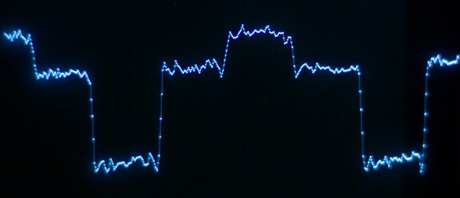
Analyzer with 500mV full scale and 40x preamp:
PCM56 8x os Yamaha CDX-5000 good adjusted MSB track 15
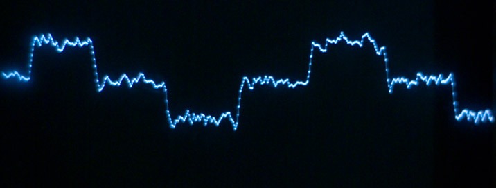
PCM56 8x os very bad adjusted MSB track 15
Dear maxlorenz
most of us are not native english speakers, but I think that
"creating the best DAC that can be made with the TDA1541 chip"
would be "Building the ultimate TDA1541A DAC" 😉
most of us are not native english speakers, but I think that
"creating the best DAC that can be made with the TDA1541 chip"
would be "Building the ultimate TDA1541A DAC" 😉
Remarks like this are totally expendable.Unless you love to see your name written...
What a debate.... Regardless of semantics, since the thread has been about the tda1541a since 2006, I think we can safely assume it is about the tda1541a...
😕 A simple thought; suppose a DAC chip has a maximum output of 2 volts and there is a noise level of 1mV, then all resolution from bit 11 would be masked in the noise level? In other words; is it the noise level in a DAC circuit that matters with how many bitresolution we leave the dac?
- Home
- Source & Line
- Digital Line Level
- Building the ultimate NOS DAC using TDA1541A