Just looking at your build.
Did it really need a heatsink that size ?
I'll be using a 20-0-20 Transformer (because that's what I've got).
Am I correct in thinking that the two MOS-FETs closest to the rectifiers will be dissipating :-
((20 x 1.414) - 10) x Iout.
If I use Iout = 200mA
That leaves me dissipating 37W x 2 of course.
I think I've just answered my own question, I got 4W first time round.
37 W x 2 so 74 W in total for a device existing out of 4 JFETS ( drawing the current of a single LED in each channel) and some resistors that can be fed with a 2 x 12 V 7 VA transformer ?!?! Do you think that is really necessary ?
Last edited:
It does seem like using a Sledge Hammer to crack a nut.
Buzzforb is driving his DCB1 with 1A. I'm not going that high.
It does ask the question though, and I agree with you Jean-Paul. What is the extra current actually doing ?
Only 10mA or so is actually being used by each channel of the B1.
Buzzforb is driving his DCB1 with 1A. I'm not going that high.
It does ask the question though, and I agree with you Jean-Paul. What is the extra current actually doing ?
Only 10mA or so is actually being used by each channel of the B1.
You need to modify the output relay for grounding at rest position too.
That seems a torturous routing for the 0V track.
I've taken a simpler route. Can't see that it makes any difference as its disconnected once the DCB1 is running.
You'll notice that the routing for the relay drive transistor has also been changed to accomodate the TIP122.
Attachments
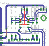
That seems a double layer PCB rather.🙂 If you will get any noise at the amp when relay is at rest position then you know. If not, all well.
*3.7W not 37W.
*3.7W not 37W.
That seems a double layer PCB rather.🙂 If you will get any noise at the amp when relay is at rest position then you know. If not, all well.
*3.7W not 37W.
So I was right in my first calculation.
Why has Buzzforb used such MASSIVE heatsink.
Last edited:
That seems a double layer PCB rather.🙂 If you will get any noise at the amp when relay is at rest position then you know. If not, all well.
*3.7W not 37W.
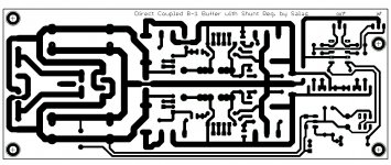
The original layout was for a single sided board.
Did you poduce a board with a ground plane on the upper side.
My B1 is Double Sided but there are no traces on the upper side.
Would I be better with a double sided board, simply keeping all traces on the bottom side and the 0V on the upper side ?
We use a double layer plated through board later indeed. The red traces look so. You can do it in single layer, you miss a couple of jumpers in the one you showed to mimic I think.
So I was right in my first calculation.
Why has Buzzforb used such MASSIVE heatsink.
I have compensation issues😀 It does provide a useful reference. If mounting under th board, you will need about a 4" x 8" area for the board. That heatsink only gets lukewarm at 1A and yes, it does make a difference. Remember not to assume things. The only reason i didnt try 2A is because my trafo couldnt take it. Heatsinks may not be able to take it. I cant wait till you hear what "little" difference there is from this and regular B1
We use a double layer plated through board later indeed. The red traces look so. You can do it in single layer, you miss a couple of jumpers in the one you showed to mimic I think.
Of course. All I showed was the trace layout.
I have compensation issues😀 It does provide a useful reference. If mounting under th board, you will need about a 4" x 8" area for the board. That heatsink only gets lukewarm at 1A and yes, it does make a difference. Remember not to assume things. The only reason i didnt try 2A is because my trafo couldnt take it. Heatsinks may not be able to take it. I cant wait till you hear what "little" difference there is from this and regular B1
What is the extra current actually achieving ?
The B1 only consumes the Idgs current of the 2SJ170 which is approx 10mA.
The B1 is pretty immune to PSU noise so it cant be down to PSU noise.
I'm not criticizing, I believe there may well be a sonic difference. I'm just inviting comments as to why.
I've got a standard B1 with a low impedance power supply and it sounds wonderful. I'll use any comments to see how my DCB1 compares with my B1.
I was going to rip the B1 apart for components for the DCB1 but Im going to keep them both to compare them. Other than the output caps.
Did no-one have any comments about using the BYW80-150 diodes.
I suppose there are loads of High Speed diodes that will all do the job equally well in this case.
I suppose there are loads of High Speed diodes that will all do the job equally well in this case.
use byv79, i think , andit works fine. I dont know that i know enough to explain it, but i wouls day it is similar to the idea of Class A to Class b. You simply have more in teserve to meet the demands. I believe shunt is like semi ideal ccs, maintaining as constant a voltage and current as posiible and just throwing away the rest.
Changing the CCS current changes the Id of both the big mosFETs.
Transconductance of mosFETs depends very much on Id.
MosFETs run at low Id do not amplify well (due to low transconductance).
That's why I was surprised to see irfp240 being specified for the first DCB1.
It was asking the wrong devices to do the two jobs being asked of them.
That is why we now see/hear performance changing when we change currents.
We are moving the devices onto different parameters/characteristics.
The various Salas Shunt Regulators that followed the DCB1 were designed to perform with better layouts and better devices.
Last edited:
No, I would suggest that reading the development of all the variants that followed the DCB1 and applying those lessons to the DCB1, will result in a better performing regulator.
But, will that result in a better performing B1 without the coupling caps?
But, will that result in a better performing B1 without the coupling caps?
I'm not brave enough to drive a powerful Aleph DC coupled with a DC coupled pre-amp with no protection.
look at the datasheet curves.Wouldn't increase rail voltage provide similar benefit of increased transconductance.
I remeber nelson and Juma talking about higher Vds and its affect on performance. I believe the topic centered on capacitance and miller effect, but i seem to recall them saying that increasin gthe Vds had the effect both linearizing the response as well as making it easier to drive, similar at least to increasing the Ids.
- Home
- Amplifiers
- Pass Labs
- Building a symmetrical PSU B1 buffer