It has a minimum drift of the output voltage when the temperature changes. With it, you can refuse the input capacitor of the main circuit.
A few pics..
Hi amplitud
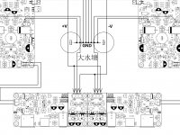
Can you share a wire interconexion pcb diagram?
Thanks.
Hi Friends, what fuse for system use?
It's dependent on the components you used in your powersupply...
It's dependent on the components you used in your powersupply...
I bought the same to you.
2xamp Pcb+ input pcb + psu pcb
It seams Input work with 33v and the v2 input is from amp pcb v2 output?
A wire diagram between the pcbs will help me a lot
Thanks.
All documentation is already available in this thread, somewhere.
I bought the same to you.
2xamp Pcb+ input pcb + psu pcb
It seams Input work with 33v and the v2 input is from amp pcb v2 output?
A wire diagram between the pcbs will help me a lot.
the documentation shows the input pcb is feeded from the same dc output to feed the amp pcb, this would be 65vdc.
Attachments
The middle part of input pcb is a dual voltage regulator, it delivers the 33 volts as needed.
so what is for the +-V2 (33v) output from amp pcb?
Good question. But if you're thinking of feeding input pcb with those mentioned +/÷ 32 volt, I'm not sure the regulators can handle the extra current, maybe chalky knows, but follow the schematic and you're good, try your alternative and it's on you.

Last edited:
A few pics..
Hi, did you conect the 18VAC input in the protect ciruit from another transformer?
c16 -c17?
Hi Chalky, why you didin´t install c16 and c17?
Finally got back to work on my 4bsst klone - got interrupted by a nasty bout of genuine influenza. I finished the input board and everything tested fine. There's a small gotcha if you test the input board by itself - the signal ground and the stabilised power supply ground are not connected on the pcb. So if you, like me, use a floating power supply as input to the pcb stabilised power supply then there is no common ground and the input board does not work. A temporary wire bridge fixes this. The overall gain of the input board from the phono input is x2 not x3 a I previously stated.
The discrete component opamp has a gain of x3 but there is x0.667 attenuation at the input so overall the gain is x2. The real Brystons have their phono input sockets attached to the pcb and not the metalwork, so there is a point of weakness. The klone phono sockets are soldered to the pcb but also have mounting nuts to fix them to the back panel, so no weakness there. You can see this in the attached photograph. I ran a quick fft spectrum analysis with the input board producing a 1v rms output at 1kHz and any distortion was lost in the noise. I probably could have dug distortion out of the noise if I averaged for long enough but with a figure of well under -100dB I wasn't inclined to bother.
As well as documenting my build of the Bryston 4bsst klone I intend to redesign both the input board and the power amp board. The power supply and protection board will remain unchanged. Why bother to do this when I'm sure the klone will measure and sound fine? Well the input board and the input/vas of the power amp board use a common discrete component symmetrical opamp design which performs fine, but can definitely be improved. The opamp has npn and pnp input long tailed pairs and the collector currents of neither pair perfectly balanced - close, but far enough apart to give rise to small extra distortions.
The choice of push pull vas transistors in the power amp is sub optimal and suitable replacements will yield further small reductions in distortion, particularly at hf. The thermal tracking of the Vbe multiplier needs some investigation ( it may be ok ) and the circuitry around the quiescent current setting potentiometer needs to be put back to something resembling the Bryston original. Otherwise its far too easy to blow up the output devices unless the pot is set correctly before switch on. I'll redraw the original discrete component opamp circuit and aslo sketch out some alternatives. For the moment I intend to leave the output stage of the power amp as it is.
Hi Chalky, why you didin´t install c16 and c17?
Look closely at schematic, theres a dot, referring to optional if instability occurres, you are talking about input board yes?
yes, in input pcb.
in my bom list it didn´t even appears those caps, but in the pcb they appears.
in my bom list it didn´t even appears those caps, but in the pcb they appears.
Got perfboard prototype of the solid state relay for loudspeaker protection finished today. It uses an Avago ASSR-V621-302E photovoltaic opto coupler together with a pair of FDP083N15A mosfets ( 150 V, 117 A, 8.3 mΩ ) in the "standard" circuit found all over this forum. The ASSR-V621 leds are connected in series and the photovoltaic outputs in parallel. I use a 680R series resistor to give a led current of 15mA. The polarity of the coil connections to the relays is immaterial for mechanical types but it matters for the solid state version. Unfortunately the designer of the main power supply/protection pcb has not been consistent in his choice of coil polarity connections and so two versions of the solid state relay are required - each with a different polarity for the "coil" connection. The module simply drops into the pcb in place of a mechanical relay.
How does it sound? Will it bring more degradation to the signal?
The mosfets don't degrade the sound. The difference in thd between the amp output and the amp output via the mosfets is almost immeasurable. Plenty of people say they can't hear any difference when a ssr loudspeaker protection is inserted into the amplifier output. I can't hear any difference either but then I'm old enough that my hearing ain't what it used to be.
Last edited:
- Home
- Amplifiers
- Solid State
- Bryston 4B SST clone