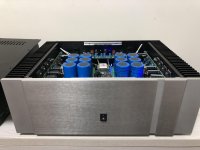
Hard to see solid state relay used in amps, few model of Accuphase amp maybe, I'm willing to take a shot , and here is my build: +/-83v,DC couple.
, and here is my build: +/-83v,DC couple.Attachments
Last edited:
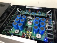
Nice build swing. I'd put some heatsinks on top of the bridge rectifiers if I was you - they run hot if you push the amplifier hard. In answer to an earlier question about +V2 and -V2 these are not 33V rails but lightly filtered versions of the full rail voltages +V1 and -V1. Can't really see any use for them.
Very nice build, congratulations, are you satisfied with audio reproduction?
This machine very sensitive, if you change the electrolytic capacitors even the internal power wire (that I can't explain why), you can feel the differences, I spent months to experiment and adjust, now it sound better, my friend said those electrolytic capacitors beside the power transistors should not be installed(Rubycon ZLH 470uf/100v in my case), it made the 'live feeling' worse, but I still keep it in the place, hard to disassemble
 ...
...Nice build swing. I'd put some heatsinks on top of the bridge rectifiers if I was you - they run hot if you push the amplifier hard. In answer to an earlier question about +V2 and -V2 these are not 33V rails but lightly filtered versions of the full rail voltages +V1 and -V1. Can't really see any use for them.
The bridge rectifiers are ok, I put this amp in my reading room, not much chance to turn it loud, but the heatsinks on the power adjust transistors in the input board got very hot, it can go above 80 degrees Celsius in summer, make me nervous, I must find a way to put a bigger heatsink on, the new vesion of clone has improve.
Swing you don't necessarily need bigger heatsinks on the input board. You could put 24-33V 5W, say, zeners in series with the power inputs to the board. This way the zeners would share the dissipation with the pass transistors on the input pcb. The problem arises because of your +/-83V supply voltage which gets dropped to +/-33V by the pass transistors on the input board. That's 50V across each of them with a current draw of around 20mA so the dissipation is approximately 1W into a small heatsink. So the heatsinks get very hot. An alternative to what I suggested above is to fit a larger heatsink underneath the input board and bolt the pass transistors to this with their legs sticking up at right angles into the pcb.
Thank you Clalky, put the heatsink underneath the input board is a brilliant idea, there much room for it, zeners still have heat dissipation issue and hard to deal with.
chalky sorry for misspelled your nickname, can't edit #_#
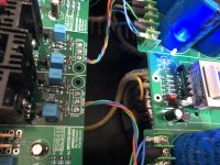
I was thinking change the amp board R2(1.2K) to a higher resistance, say 10K, the lower resistance good for noise reduce, but lack of rhythm.
I was thinking change the amp board R2(1.2K) to a higher resistance, say 10K, the lower resistance good for noise reduce, but lack of rhythm.
The input to the power amp is a bit odd with the suggested value of 1.2k because it attenuates the input to a third of its original value. If you made R2 4.7k you'd get less attenuation and probably reduce the output offset ( R14=R2+R3 approx. )
How does it sound? Will it bring more degradation to the signal?
Of course it will. Harder to say if better or worse than a relay, as relays vary greatly. Perhaps a large number of parallel trench mosfets may work, but single ones were unacceptable to me. Ymmv.
On the plus side, unlike relays, mosfets actually work when there is a fault condition.
Last edited:
I use DC couple between input board and amp board, now output offset is 0.3mV(L) and 1.3mV(R),mostly cause by zeners tolerance(31V~34V), that is acceptable for me. But the input board R20(1.5K) parallel with the amp board R2(1.2K), definitely a heave load, if change to 10K+10K, THD will slightly improved in simulation, at least the output transistors on the input board still stay in A class when large dynamic comes.
Attachments
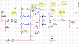

Hi..all just started to complete 4b after long silence period.I strictly followed the debugging procedure as mentioned in instruction but bias voltage (Voltage across r45) suddenly rising after few seconds, is it self excitation? Will resolve with c12,c13 alteration? Any other causes? Any fellow with same experience? Please help me
Thanks
Thanks
Hi..all just started to complete 4b after long silence period.I strictly followed the debugging procedure as mentioned in instruction but bias voltage (Voltage across r45) suddenly rising after few seconds, is it self excitation? Will resolve with c12,c13 alteration? Any other causes? Any fellow with same experience? Please help me
Thanks
I could not see the previous discussion with same problem...Trampo how did you get resolve your problem ...by changing c12,c13 .?
Many thanks Amplidude.....resolved the problem with changing to 150pf.I adjusted voltage to 12ma across R45 and switch of the amp and switch on again voltage was around 9mv..done this several times but always voltage was below the adjusted level why is that ?
I want to use this amp in small hall party occasions so please let me know how to increase gain of the AMP,....any changes in feedback? Already I am using a input module .
I want to use this amp in small hall party occasions so please let me know how to increase gain of the AMP,....any changes in feedback? Already I am using a input module .
Glad you got it fixed. I also changed C12 and C13 from 100pF to 150pF and is all good. The amp has been used every day for the last couple of months without any problems.
I use DC couple between input board and amp board, now output offset is 0.3mV(L) and 1.3mV(R),mostly cause by zeners tolerance(31V~34V), that is acceptable for me. But the input board R20(1.5K) parallel with the amp board R2(1.2K), definitely a heave load, if change to 10K+10K, THD will slightly improved in simulation, at least the output transistors on the input board still stay in A class when large dynamic comes.
The noise shelf will rise significantly. How is the temperature of Q5Q6?
I tested the input module with a load of 1.5 kOhm. More correct meander with input C1S2 220-270pf.
Worried about hot input module Q5Q6. Even with radiators hot. Can change to T126?
I am also having same problem...hot to Tuch....I thank chalky is investigating for this issue?
- Home
- Amplifiers
- Solid State
- Bryston 4B SST clone