Hello Bob,
Congrats on wonderful piece of work, your book must be refreshing and interesting as it contains special "chocolate" for Mosfet amplifier lovers like me🙂.
I would like to ask you about one thing:-
Does this book contains some flavour on N-channel output stages and distortions figures and associated plots?
Cheers...!!!
Kanwar
Hi Bob,
I was referring to the data from Nelson Pass.
(I knew already that you are using 2SK1530/2SJ201 verticals 😉).
BTW, what are your favorite MOSFETs? Mine are the Toshibas, but I've also ordered a bunch of FQA12P20/FQA19N20* pairs, but not yet tested them.
Cheers,
E.
* Not the C version (FQA19N20C), which has a much higher Cgd.
PS: Thanks Gaetan.
Hi Edmond,
My favorites are also the Toshiba 2SK1530/2SJ201. They are fairly well-matched, have a more conveniently low Vgs, and are in that nice big TO-264 package. However, they are quite a bit more expensive than other verticals.
I must admit that I have not tested the FQA12P20 and FQA19N20.
Over the years, most of my experience has been with the IRFP240/9240.
Cheers,
Bob
favorite MOSFETs ? not yet tested.
The J201/K1530 may be the current Rolls of Vertical MOSFET audio power devices, on the top-10 price list.
In a practical sense, they have the ease of matching edge, compared to price breakers from Fairchild.
=> http://www.diyaudio.com/forums/grou...oup-buy-fqa19n20c-fqa12p20-5.html#post1558243
Mr Stuart must be a Cgs lover.

[snip][
Mr Stuart must be a Cgs lover.
Surely you must be joking Mr Vermeulen. 😀
Cgd is a real PITA. You can't compensate for it, as it is a moving target you always will miss.
I joke a lot, especially for 70 €cent a pop selected.
Cgd of Toshibas is not exactly pretty either, in particular for the junior versions that i've often used for economical reasons.
All things relative : http://www.diyaudio.com/forums/pass-labs/129040-mosfet-output-stage-capacitance.html#post1599135
(admit i still have quite a number of power Laterals for a simple minded. For a scary moment, check out Cgd/Cgs of the NEC J135 )
Cgd of Toshibas is not exactly pretty either, in particular for the junior versions that i've often used for economical reasons.
All things relative : http://www.diyaudio.com/forums/pass-labs/129040-mosfet-output-stage-capacitance.html#post1599135
(admit i still have quite a number of power Laterals for a simple minded. For a scary moment, check out Cgd/Cgs of the NEC J135
)Hello Bob,
Congrats on wonderful piece of work, your book must be refreshing and interesting as it contains special "chocolate" for Mosfet amplifier lovers like me🙂.
I would like to ask you about one thing:-
Does this book contains some flavour on N-channel output stages and distortions figures and associated plots?
Cheers...!!!
Kanwar
Hi Kanwar,
Thank you for your kind words and I am glad that you like the fact that it has a significant amount of MOSFET content.
By N-channel output stages I presume you mean all-N-channel output stages, those that typically are of the quasi-complementary architecture. Unfortunately, I do not include any material on quasi-complementary all-N-channel output stages.
While I respect the opinions of others, my own feeling is that they are not a good design approach. Price and availability of P-channel devices is not really a factor pushing one to quasi-complementary approaches (as it was in the early days of BJT output stages). The other argument I have heard in support of quasi-complementary all N-channel output stages is that they benefit from the fact that the transistors used in the top and bottom halves of the output stage are of the same type and have more nearly identical characteristics. Unfortunately, the very different way in which the devices are used in the top and bottom halves makes for very serious differences in the behavior of the top and bottom parts - far worse than the systematic differences one finds between N-channel devices and P-channel devices.
Cheers,
Bob
How very true , I just made the design choice of going complimentary just for that reason. One can always compensate for a slight difference in device characteristics rather than using an unbalanced topology.
OS
OS
Surely you must be joking Mr Vermeulen. 😀
Cgd is a real PITA. You can't compensate for it, as it is a moving target you always will miss.
I agree, Cgd can be a problem in several regards. It can climb to a very high value when the signal approaches the rails and significant current is being driven into the load, since it gets larger with smaller Vgd reverse bias. The forward gate bias required to source high current only makes things worse.
It can easily climb to 1000 pF for an IRFP240 under some conditions. It gets proportionately worse when multiple pairs of output devices are used. This is one reason that we cannot be complacent about the drivers for MOSFET outputs - they have to pull out charge, not unlike drivers for BJTs. However, for MOSFETs and sinewaves,the highest voltage slew rate typically occurs at an output voltage where Cgd is fairly small. However, a squarewave presents a much worse condition, and cross-conduction can occur when the MOSFET output is pulled away from the rail at a high rate of change.
There is also another problem: parasitic oscillations. We all know that MOSFETs are fast and are sometimes prone to local parasitic oscillations in the VHF band. Cgd often plays a role in the creation of the oscillator topology and resonance that is the root cause of the parasitic oscillation.
With Cgd moving around with signal, changing in value by an order of magnitude, many more signal-dependent opportunities for parasitic oscillation are presented.
Finally, do not overlook the fact that Ccb for BJT output transistors can also get pretty ugly.
Cheers,
Bob
Hi stinius,
These are very good questions.
I've done spot checks, but no plots, for both source resistors the same, and both source resistors at 0, all with each pair biased at 165 mA. But not plots.
The biggest reduction is in 2nd harmonic, while the reductions in other harmonics are modest. For example, at 20V peak into 8 ohms, around the intermediate power THD peak, 2nd went from 0.12% down to 0.021%, when 0.33/0.15 ohms was used instead of 0.22/0.22 ohms.
3rd went down from 0.026 to 0.024, while 5th went down from 0.0065 to 0.0041. 7th actually went up from 0.0001 to 0.00024, but these numbers are very low in the first place, and only represent a single power data point.
With respect to the distortion simulations, I did it with both no gate stopper and 47 ohm gate stopper and there was essentially no difference in distortion. In amps that I have built, I have done very little experimenting with different gate stoppers. I usually use 47 ohms and a gate Zobel network with vertical MOSFETs, much as I did 25 years ago when I did my MOSFET power amp with error correction.
Hope this answers your questions,
Cheers,
Bob
Hi Bob
Thank you for your answer, it coincides with what I have found.
BTW: I have been playing around with different resistor values with different topologies and found something interesting, as an example the 7th was halved.
Cheers
stinius
Hi Bob
BTW: I have been playing around with different resistor values with different topologies and found something interesting, as an example the 7th was halved.
Cheers
stinius
Hello Stinius
Is the 7th halved in simulation or actual measurements
Arthur
Hi Kanwar,
Thank you for your kind words and I am glad that you like the fact that it has a significant amount of MOSFET content.
By N-channel output stages I presume you mean all-N-channel output stages, those that typically are of the quasi-complementary architecture. Unfortunately, I do not include any material on quasi-complementary all-N-channel output stages.
While I respect the opinions of others, my own feeling is that they are not a good design approach. Price and availability of P-channel devices is not really a factor pushing one to quasi-complementary approaches (as it was in the early days of BJT output stages). The other argument I have heard in support of quasi-complementary all N-channel output stages is that they benefit from the fact that the transistors used in the top and bottom halves of the output stage are of the same type and have more nearly identical characteristics. Unfortunately, the very different way in which the devices are used in the top and bottom halves makes for very serious differences in the behavior of the top and bottom parts - far worse than the systematic differences one finds between N-channel devices and P-channel devices.
Cheers,
Bob
Hi Bob,
Thanxz for replying🙂
Yes, i was referring to all N-channel output stage. Though i wont indulge in any sort of argument as i also respect opinion of others.
In N-channel output stages generally we have CD at upper side and CS at lower side which makes huge difference in open loop output impedances of both halves, whereas in complementary this difference is very less, but then again we have drastic differences in complementary vertical mosfet outputs.
such as:-
1) input capacitance,
2) trans-conductance,
3) output capacitance
4) RDS
These differences donot exist in non-complementary outputs.
Though both have pros/cons, its more or less dependent on recipe of designer and of course power requirements.
BTW: Local feedback helps alot in All N-channel output stages
regards,
Kanwar
Attachments
Hi Bob,
Thanxz for replying🙂
Yes, i was referring to all N-channel output stage. Though i wont indulge in any sort of argument as i also respect opinion of others.
In N-channel output stages generally we have CD at upper side and CS at lower side which makes huge difference in open loop output impedances of both halves, whereas in complementary this difference is very less, but then again we have drastic differences in complementary vertical mosfet outputs.
such as:-
1) input capacitance,
2) trans-conductance,
3) output capacitance
4) RDS
These differences donot exist in non-complementary outputs.
Though both have pros/cons, its more or less dependent on recipe of designer and of course power requirements.
BTW: Local feedback helps alot in All N-channel output stages
regards,
Kanwar
Hi Kanwar,
It usually boils down to which dragon each engineer is willing to slay. A good designer can certainly mitigate the problems of a quasi-complementary output stage. Other designers are better able to mitigate the N vs. P-channel differences you list.
Cheers,
Bob
pre-ordered this as well (along with nearly 200quid of other audio/electronics/loudspeaker texts); I haven't built anything yet and this hobby has started to get pricey (it was already time consuming) 🙂
M Cordell
I ordered my copy to be shipped on 1 december
I have two questions:
First do you expect simulation to be accurate enough to make comparison between designs at the level of distortion we are talking ( 0.001). Distortion components are depending on derivatives which is very sensitive to model variations.
Did you read the book from Sansen: Analog design essentials. Very interesting practical and in depth approach on design short cuts and models but mainly cmos integrated circuits. A lot is still valuable in general. Very interesting and new approach of teaching and book writing.
I experienced exactly what you said on people having somme initial difficulties in grasping in depth but then by far better in explaining which is leading to even better understanding.
Some consultants have made an international network of teaching ( like Don White in EMC). Why should you not start a network of teachers based on your book. It is missing and would attract attention with your reputation in the field. I am interested.
JPV
Ccb for BJT output transistors can also get pretty ugly.
Reminds me of an '82 Burmester design : 120W Toshiba RET drivers for 3 pairs of 200W Sanken A1216/C2922 output devices.
Hi Kanwar,
It usually boils down to which dragon each engineer is willing to slay. A good designer can certainly mitigate the problems of a quasi-complementary output stage. Other designers are better able to mitigate the N vs. P-channel differences you list.
Cheers,
Bob
I duly agree Bob...!!!🙂
I think Toshiba vertical complementary pairs are much better in performance and specs then IRF 240/9240 counterparts.
Goes for the baby Tosh too, and up to 50% cheaper per W power handling.
<10ppm (1W) and 50W continuous on a single output pair.
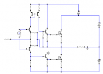
Elegant circuit, including the power supply/biasing!
jd
M Cordell
I ordered my copy to be shipped on 1 december
I have two questions:
First do you expect simulation to be accurate enough to make comparison between designs at the level of distortion we are talking ( 0.001). Distortion components are depending on derivatives which is very sensitive to model variations.
Did you read the book from Sansen: Analog design essentials. Very interesting practical and in depth approach on design short cuts and models but mainly cmos integrated circuits. A lot is still valuable in general. Very interesting and new approach of teaching and book writing.
I experienced exactly what you said on people having somme initial difficulties in grasping in depth but then by far better in explaining which is leading to even better understanding.
Some consultants have made an international network of teaching ( like Don White in EMC). Why should you not start a network of teachers based on your book. It is missing and would attract attention with your reputation in the field. I am interested.
JPV
Hi JPV,
The validity of distortion simulations can vary quite a bit depending on the quality of the models. With good models, I do believe that apples-apples comparisons of the distortion characteristics of two different circuits using the same devices and models will usually be fairly reliable in telling which circuit is better, even at low distortion levels. Comparisons of two circuits that are quite different will likely be less valid.
The bottom line is that simulations are well less than perfect, but very valuable nonetheless. Bear in mind that distortion, especially in the ppm range, is often governed in the physical implementation of the amplifier by things that are not simulated.
There is no replacement for building and measuring the final amplifier, but those measurements must also be carried out with great care, and are also subject to errors in telling which amplifier circuit is better.
Willey Sansen is a very old friend of mine, but I am embarrassed to say that I don't think I have read that book. He and Bob Meyer were two of my heros back when I was learning a lot of this stuff.
I would love to start a network of teachers teaching courses based on my book. Although I would not rule out 4-year colleges (Marshall Leach teaches a great course based on his book at Georgia Tech.), I think there would be really good appeal at community colleges and audio engineering vocational schools. Here the value-added is in being able to teach students electrical engineering who might otherwise not be interested in it. Designing and building amplifiers is the hook that can get them interested in it, rather than having to study a dry course full of theory and equations.
Best regards,
Bob
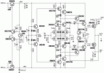
Goes for the baby Tosh too, and up to 50% cheaper per W power handling.
<10ppm (1W) and 50W continuous on a single output pair.
This is a nice circuit. Folded cascode, Miller Input Compensation. Probably very good slew rate.
The smaller 2SK1529 and 2SJ200 are, price-wise, a fairer comparison to the IRFP240/9240, since both are in the smaller T0247 package. The nice big TO-264 package of the 2SK1530/2SJ201 probably accounts for the higher price.
I personally really like parts in the larger TO-264 package, not just for the often higher device rated power dissipation, but for the much higher metal header-to-heat-sink contact area, reducing the thermal resistance of the transistor insulator.
BTW, any further news on the so-called obsolescence of the 2SK1530? Digikey says so, but I have not seen other evidence of it. Also, Digikey does not say that about the 2SJ201.
Cheers,
Bob
- Home
- Amplifiers
- Solid State
- Bob Cordell's Power amplifier book