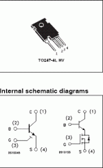
heard of ESBT
Gee, they've only been around for 10 years or so.
Aren't they scary expensive? A quick look in a local online catalog shows quite a few cheap but usable devices e.g:
- MOSFET 1500V: $5
- BJT 1500V Vce: $2
- IGBT 1700V: $4
- ESBT 2200V: $6
How about that - I just learned something by mistake. I'd never heard of ESBTs before. 😱

Hi Godfrey,
I don't recall hearing of an ESBT before either. What are they and what does ESBT stand for? Electro-Static Bipolar Transistor???? 🙂.
Cheers,
Bob
Hi Godfrey,
I don't recall hearing of an ESBT before either. What are they and what does ESBT stand for? Electro-Static Bipolar Transistor???? 🙂.
Cheers,
Bob
I found this link http://www.st.com/stonline/books/pdf/docs/12830.pdf
Maybe it is this. Hybrid emitter switched bipolar transistor. ESBT.
David.
Low THD amps
Hello Bob
Another quetion about construction, I agree with the ouput inductor being placed away from the main amplifier PCB because power supply magetic fields can couple signal, but my question is how far away to you do try to place the amplifier high power signal exit point from the power supply entry leads.
Regards
Arthur
see forgotten attachment 🙂.
Hi Bob,
I ran your MOSFET LF Anomalies test on a sample Vishay IRFP9240 and I do not see the issue:
100 Hz 26.0 mV in .60 V out
10KHz 25.94 mV in .593 V out
I used a 10 ohm load resistor since that is what I had handy, with a 20V power supply biased at 1A. I built it exactly as shown but with a 10 uF input coupling cap since it is what I had handy. I only bypassed the main supply with .1 uF.
You used a 10K resistor in series with the generator and you need the 100 ohm to ground to provide a low source impedance. I was getting attenuation similar to yours when I didn't use the 100 ohm shunt. 10K seems high since you really have to run up the generator to get 26 mV.
I'm really surprised with the results since Vishay bought IRs Power Division but perhaps they were making their own version of the part before the purchase. Or perhaps I'm doing something wrong, but I doubt it - checked it several times.
Last edited:
Hi Bob,
I ran your MOSFET LF Anomalies test on a sample Vishay IRFP9240 and I do not see the issue:
100 Hz 26.0 mV in .60 V out
10KHz 25.94 mV in .593 V out
I used a 10 ohm load resistor since that is what I had handy, with a 20V power supply biased at 1A. I built it exactly as shown but with a 10 uF input coupling cap since it is what I had handy. I only bypassed the main supply with .1 uF.
You used a 10K resistor in series with the generator and you need the 100 ohm to ground to provide a low source impedance. I was getting attenuation similar to yours when I didn't use the 100 ohm shunt. 10K seems high since you really have to run up the generator to get 26 mV.
I'm really surprised with the results since Vishay bought IRs Power Division but perhaps they were making their own version of the part before the purchase. Or perhaps I'm doing something wrong, but I doubt it - checked it several times.
Hi Pete,
Thanks for doing these measurements. Sounds like you've got it right, and this is really great news. I'm guessing that Nelson Pass will also be interested in these results.
The disappearance of the anomaly could be due to a number of different things. I too am surprized to see it gone. I'm guessing it was some minor defect in the process and that even without an explicit process change perhaps better processing over time reduced it, even if it is still made with the IR process.
Thanks again.
Cheers,
Bob
Hi Arthur,
This is a good question and of course subject to YMMV. In my MOSFET power amplifier with error correction I got to below 0.001% THD, and the influence of the half-wave class AB output currents was probably below that.
Getting the influence of those currents way down involves great care and attention to detail in layout. For example, when I use multiple output pairs, I interleave the P and N devices rather than group each sex together. This helps with some cancellation of the created magnetic fields. I also try to take advantage of the fact that in such amplifiers the sum of the positive and negative rail currents is essentially linear, so twisting together the + and - rail leads helps cancel the fields there. I also try to strongly AC short the positive and negative rail at the output stage with capacitors that straddle the rails in order to get those currents summed together as locally as possible.
It is also important to keep that influence away from the feedback path. I send the full-amplitude output signal back to close to the input stage, where I then have the feedback network.
It is also very important to pay attention to grounding and not allow these half-wave currents to corrupt the ground, espcially the quiet ground. Also be aware that power supply bypass capacitors can corrupt a ground by bypassing these half-wave rectified rail noises into the ground. Overall, grounding practices are very important in this regard.
Cheers,
Bob
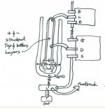
Bob,
I like to draw up diagrams to try out layouts before spending a lot of time with the PCB software. I drew up the attached to see if I could turn your words into a picture. I haven't shown the P devices, but they would be mirror image of the N's on the left side of the power. I've stacked the + & - on the top and bottom layers of the board, an ringed them with ground. The feedback would be shielded wire with the ground connection for the shielded wire being at the other VAS end where there is clean ground. Other changes might be moving the inductor off board. What do you think? Does this make sense, or should the + & - be side by side with the ground below both of them?
Thanks
Ken
p.s. I goofed up the post and will have to attach the image in the next post.
Last edited:
I found this link http://www.st.com/stonline/books/pdf/docs/12830.pdf
Maybe it is this. Hybrid emitter switched bipolar transistor. ESBT.
David.
Very interesting part. However, look at Figure 12, the reverse-biased SOA curve - the chart is blank.
It is a bit unclear how this device would fare in a linear application with regard to SOA. Maybe I'm missing something in the datasheet.
Cheers,
Bob
Hello Bob
Another quetion about construction, I agree with the ouput inductor being placed away from the main amplifier PCB because power supply magetic fields can couple signal, but my question is how far away to you do try to place the amplifier high power signal exit point from the power supply entry leads.
Regards
Arthur
Hi Arthur,
First, bear in mind that there are two reasons to keep the output inductor away from the small-signal parts of the circuit and from the power leads. The first is to avoid inducing noise from the power supply leads into the inductor. The second is to keep magnetic fields created by audio signal currents in the inductor from getting coupled into the small-signal stages of the amplifier.
I don't try especially hard to keep the power output lead far away from the power supply rail wires, but I certainly try not to run them parallel to each other over any significant distance.
Cheers,
Bob
Bob,
I like to draw up diagrams to try out layouts before spending a lot of time with the PCB software. I drew up the attached to see if I could turn your words into a picture. I haven't shown the P devices, but they would be mirror image of the N's on the left side of the power. I've stacked the + & - on the top and bottom layers of the board, an ringed them with ground. The feedback would be shielded wire with the ground connection for the shielded wire being at the other VAS end where there is clean ground. Other changes might be moving the inductor off board. What do you think? Does this make sense, or should the + & - be side by side with the ground below both of them?
Thanks
Ken
p.s. I goofed up the post and will have to attach the image in the next post.
Hi Ken,
I like the idea of the plus and minus rails being stacked one on top of the other on top and bottom layers. Which layer is the ground on? It sounds like your plan has the feedback cable's center conductor and shield straddling much of the output stage. This is probaly not a good idea if I understand it correctly. I would ground only one end of the feedback shielded cable and that would be the end near the input stage. I'd probably also lean toward a design that gets the P side and N side output transistors next to each other rather than across from each other. I also like to put the temperature sensing diode between the two output transistors (or in the middle of an array of several output transistor pairs). Don't forget the resistor across the output coil. I think you can go either way with the coil on or off the board.
Cheers,
Bob
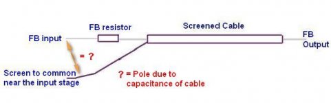
Pole etc ?
@ Bob Cordell
Hi, admittedly i havn't been able to read all the posts, or seen the circuit diagram, 🙁 so forgive me if i appear to intrude somewhat, but i felt compelled to post, if only to possibly gain some insight, as well as "hopefully" offering some.
Re -
I tend to agree, as that "might" induce more nasties than it keeps out ? A dedicated quasi smoothed common "could" be created that "might" serve that purpose ? Or just run a non screened cable, but clear of any inducements.
Wouldn't doing that negate any desired benefits, as i would have expected a driving signal to accompany a driving reference point, ie common/ground near the drive ?
Also would that not create a pole with the FB resistor ?
I'm picturing your proposed setup to look like the att.
Regards
@ Bob Cordell
Hi, admittedly i havn't been able to read all the posts, or seen the circuit diagram, 🙁 so forgive me if i appear to intrude somewhat, but i felt compelled to post, if only to possibly gain some insight, as well as "hopefully" offering some.
Re -
It sounds like your plan has the feedback cable's center conductor and shield straddling much of the output stage.
This is probaly not a good idea if I understand it correctly.
I tend to agree, as that "might" induce more nasties than it keeps out ? A dedicated quasi smoothed common "could" be created that "might" serve that purpose ? Or just run a non screened cable, but clear of any inducements.
I would ground only one end of the feedback shielded cable and that would be the end near the input stage
Wouldn't doing that negate any desired benefits, as i would have expected a driving signal to accompany a driving reference point, ie common/ground near the drive ?
Also would that not create a pole with the FB resistor ?
I'm picturing your proposed setup to look like the att.
Regards
Attachments
Last edited:
@ Bob Cordell
Hi, admittedly i havn't been able to read all the posts, or seen the circuit diagram, 🙁 so forgive me if i appear to intrude somewhat, but i felt compelled to post, if only to possibly gain some insight, as well as "hopefully" offering some.
Re -
I tend to agree, as that "might" induce more nasties than it keeps out ? A dedicated quasi smoothed common "could" be created that "might" serve that purpose ? Or just run a non screened cable, but clear of any inducements.
Wouldn't doing that negate any desired benefits, as i would have expected a driving signal to accompany a driving reference point, ie common/ground near the drive ?
Also would that not create a pole with the FB resistor ?
I'm picturing your proposed setup to look like the att.
Regards
Hi Zero D,
A short length of coaxial cable will probably be in the low picofarads. Such a small capacitance driven by a low impedance source like an output of an amplifier would be hardly noticeable. It's a shunt capacitance to ground. Now if the capacitance were on the other side of the resistor it would be significant. This is another reason why it's better to do it this way, rather than placing the FB resistor near the output and connecting through a shield back to the input.
David.
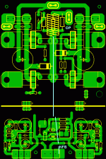
Bob,
Thanks for the critique. I revised the layout, I think this is better, but would appreciate any and all comments. The feedback trace could be a shielded wire as Bob has already described. Not everything is to scale, such as the output transistors at T-220, more of a diagram.
Regards,
Ken
Thanks for the critique. I revised the layout, I think this is better, but would appreciate any and all comments. The feedback trace could be a shielded wire as Bob has already described. Not everything is to scale, such as the output transistors at T-220, more of a diagram.
Regards,
Ken
Attachments
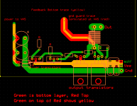
Run the OP signal on the shield, as well ... effective. I just run a stupid "purple wire" across my low imp. output board (below - blue line) , no issues. 🙂
Bob , my question is about your DBT triple (ch. 10 /page 192-3 - figure 10.6 and 10.7). You show the current sources , but what "flavor" (led , 2Q , diode). In other words , what would be the best temperature coefficient CCS to match with this excellent OP stage ? No basestoppers ? , I'll leave pads for them... I know better 😀 . Also , you run the drivers at 50ma ... is this to set a stable operating temperature for the vbe cancellation of pre/driver ?
As you see below , I will build it ... I have the all the pre/drivers separately coupled to a small PCB aluminum bar (to-126 opposes the to-220). With this much Beta , I will be able to try the hawksford cascode properly (luxman). 🙂
PS - I will initially use it as a sub amp (it might have some fidelity as well - next amp 😀 )
OS
Attachments
Ost,
in the light of these recent NFB discussions, have you felt the need to change any of your views, as we discussed some time ago?
I can't remember what we agreed on, as the final NFB scheme. Did you get measurable results for that scheme to show how well or how badly it performed?
in the light of these recent NFB discussions, have you felt the need to change any of your views, as we discussed some time ago?
I can't remember what we agreed on, as the final NFB scheme. Did you get measurable results for that scheme to show how well or how badly it performed?
Ost,
in the light of these recent NFB discussions, have you felt the need to change any of your views, as we discussed some time ago?
I can't remember what we agreed on, as the final NFB scheme. Did you get measurable results for that scheme to show how well or how badly it performed?
I did see the the slight overshoot w/ 10Khz-60V squarewave - 8R on my "bobamp" change when running the FB wire right over a rail (had to do that -worse case scenario), but changing the driver base stopper value also had that effect. At no time did anything run "badly" , maybe just not optimally . I still "like" the shielded NFB return , I just haven't had time to make one 😀 The OP coil/R on my EF2 nikko is also offboard , I can't disagree with those engineers. On my board (last post) , 40mm between rail/OP is good , have photo's/layout of a $55K luxman amp ... the OP board is similar to mine (or roenders-MJL21193's). I don't have a AP , so my "measurements" are at most ... observations and comparisons 😱 .
I won't ask bob for layout ideas , but I would really like any insight on the "DBT" - it "is" (should be - I need to build) superior.
OS
rail tracks
Hi all,
I like the discussion about the rail tracks.
First, it is very handy if you use a mirror image topology where the IPS current sources are fed from the opposite rail. Having them both on either side allows you to minimize tracks having to cross your pcb vertically to reach the other rail.
I think also that having them near eachother reduces V gradients sa they will annulate eachother to some degree. Same counts for induction fields caused by currents.
Ringing them by ground is good. I guess to use the DC decoupling ground node for this and not common ground and off-course not signal ground 🙂
Would it be wize to push the idea further?
+ : pos rail
- : neg rail
g : dc decoupling gnd
gggggggggggggggggggggggggggggggggggggggggggggg
++++++++++ ---------- ++++++++++ ----------
+ + + +
------------- ++++++++ ------------- ++++++++
gggggggggggggggggggggggggggggggggggggggggggggg
on the other side (bottom) the rails are twisted inversely.
Problem here is to get to them with your nodes?
Must be 4 layer board?
Overkill?
greetz
Olivier
Hi Pete,
Thanks for doing these measurements. Sounds like you've got it right, and this is really great news. I'm guessing that Nelson Pass will also be interested in these results.
The disappearance of the anomaly could be due to a number of different things. I too am surprized to see it gone. I'm guessing it was some minor defect in the process and that even without an explicit process change perhaps better processing over time reduced it, even if it is still made with the IR process.
Thanks again.
Cheers,
Bob
It is good to share information on these parts - to be honest I am surprised and pleased about the Vishay part. Thanks for documenting your test.
I'm looking at some N-channel only designs. I am aware of how inferior some may view them however let's say I'm considering them for a brute force subwoofer amp, and I came across the FQP46N15. It is a 46A, 150V, 210W Rds=.042 part, the capacitances are higher but it is really like 2 lower current parts in parallel. The gm is quite high at 33S. That might be a bit high on current and there is also the FQP34N20 that looks interesting.
There is a nearly comp pair: FQA36P15/FQA28N15 in TO3P package and with gms of 19.5/20S, power 294/227W - I really like this pair.
I was wondering if you've looked at these higher gm parts and if you have any opinion/experience concerning their use in audio?
- Home
- Amplifiers
- Solid State
- Bob Cordell's Power amplifier book